I wanted the TiinyAI Pocket Lab to be real.
I just finished a five-month painful journey with NVIDIA’s DGX Spark, a $3,999 “personal AI supercomputer” that turned out to be bandwidth-kneecapped to protect NVIDIA’s datacenter business. I wrote about it here. Long story short, NVIDIA hid the one number that mattered, 273 GB/s memory bandwidth, behind impressive-sounding specs like “128GB unified memory!” and “1 PFLOP FP4!” I trusted them, I bought it, I got played and I sold it at a loss.
That was a tough experience that definitely taught me not to trust marketing blindly. After being lied to once, I learnt to look for what’s not on the spec sheet. The numbers they lead with are the ones that might not matter that much, kinda like when a magician is doing misdirection. The numbers they don’t tell you are the ones that matter the most.
So after selling the DGX at a loss I was back on the horse searching for a solution that would allow me to run inference locally. Just like everyone else I wanted the biggest memory pool (ideally) for the lowest cash. That is when I found a startup called TiinyAI claiming they’d built a pocket-sized device that runs a 120-billion-parameter model at 20 tokens per second for $1,299. My first thought? Too good to be true. I opened a notepad, then I opened their website and looked at their marketing photos, their spec sheet and got to work. How does that go again? Fool me once, shame on you. Fool me twice shame on me? I was not going to be fooled twice. The first thing I thought was: 120B parameters on LPDDR5X? C’mon now. The DGX Spark has 128GB of unified LPDDR5X at 273 GB/s and I just spent five months learning why that wasn’t enough to run 70B models at interactive speeds. You’re claiming 120B on the same memory technology. What is this Voodoo magic you have…
The next few days became a scavenger hunt trying to piece together how does this device work, what is all this tech they claim to be so ground breaking and how can they defy the physics that NVIDIA were not able to fool.
What I found was three layers of technical misdirection stacked on top of forked academic research, wrapped in a corporate structure designed for opacity, and sold through a Kickstarter campaign with a $10,000 funding goal that has now raised $1.7 million from 1,266 backers.
Let’s get started.
Part 1: The Promise
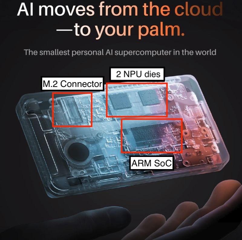
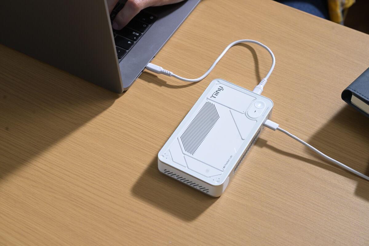
TiinyAI’s pitch is simple, the Pocket Lab is “the first pocket-size AI supercomputer.” It plugs into your laptop via USB-C, has 80GB of LPDDR5X RAM, an ARM SoC with a 30 TOPS co-located NPU, a 160 TOPS dedicated external NPU (190 TOPS total), and can run large language models with up to “120 billion” parameters locally. No cloud, no GPU, no subscription fees. Zero token costs, always on, private and offline.
The Kickstarter launched March 11, 2026. It hit $1 million from 728 backers in its first five hours. As of today, it sits at $1,737,722 from 1,266 backers, 17,377% of its $10,000 goal. The super early-bird price is $1,399. If you placed a $9.90 deposit on their website beforehand, you get it for $1,299. Estimated delivery: August 2026.
They have a Guinness World Record awarded for the “smallest mini PC (100B LLM Locally).” They were featured at CES 2026. Their press release, distributed through Hong Kong, quotes Samar Bhoj, “GTM Director,” talking about “edge-cloud synergy” and introducing “AgentBox” as a new hardware category.
The press coverage has been uniformly positive. Mashable, TechRadar, WCCFTech, Benzinga, Geo News. All echoed the “120B” and “20 tok/s” claims like parrots without doing any due diligence that would take 5 minutes and raise more questions than answers. None spent two minutes on a LinkedIn search that would have revealed the “hottest AI hardware startup in US” has four employees: a hidden VP, a GTM director with no career history, a VC analyst in Hong Kong, and a Hong Kong intern.
TiinyAI’s website and Kickstarter page now display a “Trusted by Top Media” banner listing these publications by name. Write a press release, pay for PR Newswire distribution through Hong Kong, watch outlets reprint it without fact-checking, then reference the coverage as third-party validation. This is how credibility laundering works.
I did the math.
Part 2: The Hardware They Won’t Name
What’s missing when you read TiinyAI’s marketing materials? They don’t tell you what SoC is inside the device.
Every legitimate hardware company tells you what’s under the hood. Apple tells you it’s M-series silicon. NVIDIA tells you it’s GB10. Qualcomm tells you it’s Snapdragon. Even budget SBC makers like Orange Pi and Radxa prominently name their processors. TiinyAI tells you the Pocket Lab has “an Armv9.2 CPU” and “a dedicated NPU with up to 160 TOPS.”
But they published photos. And I want to be very clear about sourcing here: every piece of hardware identification in this post comes from TiinyAI’s own publicly shared marketing materials and social media posts. Nobody leaked schematics or broke an NDA or sent me confidential docs. I looked at what they voluntarily showed the world, and I read it with 20+ years of engineering experience.
The sources, all public:
- An early prototype photo posted to social media, showing what appears to be a PCIe card inside an enclosure
- A stylized “X-ray” render posted to Twitter, showing the internal component layout including the dual-die NPU configuration and SoC package arrangement
- An exploded-view animation on their website, showing the layer stack from base enclosure through thermal interface, M.2 dNPU module, and top shell, confirming the modular two-board design
- Their own spec sheet listing “Armv9.2,” “12-core,” “160 TOPS dNPU,” and “80GB LPDDR5X,” enough constraints to narrow the silicon candidates dramatically
- The M.2 connector visible in prototype and render photos, never mentioned in their specs, but plainly visible in their own images, confirming the PCIe-attached dNPU architecture
The SoC: Process of Elimination
ARMv9.2 is bleeding-edge. Very few SoCs in production implement this ISA. I went through every candidate I could find:
Qualcomm Snapdragon X Elite: 12-core ARMv9.2. Matches the core count. But it’s Windows-exclusive silicon with heavy Qualcomm branding. If you had a Snapdragon inside, you’d market it. Eliminated.
MediaTek Dimensity 9300: ARMv9.2, but only 8 cores. Wrong count, mobile SoC, can’t support 32GB LPDDR5X. Eliminated.
Apple M-series: Custom ARM cores, not licensable, Apple-only. Eliminated.
Ampere Altra: ARMv9.0, 128-core server chip. Wrong core count, wrong power envelope, wrong ISA revision. Eliminated.
That leaves exactly one chip: the CIX P1 (CD8180) from CIX Technology, a Shenzhen-based fabless semiconductor company. It’s the only publicly announced 12-core ARMv9.2 SoC in production:
- 12-core Armv9.2 DynamIQ CPU: 4x Cortex-A720 big cores at up to 2.8 GHz (later capped at 2.6 GHz in production), 4x Cortex-A720 medium cores at 2.4 GHz, 4x Cortex-A520 LITTLE cores at 1.8 GHz
- GPU: Arm Immortalis G720 MC10 with hardware ray tracing
- Built-in NPU: 30 TOPS (Arm-China Zhouyi), supporting INT4/INT8/INT16/FP16/TF32
- Memory: 128-bit LPDDR5X bus
- PCIe: Gen4 x4 via M.2 M-Key
- Process: TSMC 6nm
My confidence level is very high, there literally isn’t another chip matching these specs.
This is not exotic hardware. You can buy this exact SoC in a Radxa Orion O6 mini-ITX board for $200-300. Minisforum sells the MS-R1 mini PC with this chip and up to 64GB of LPDDR5X for about $500-700. Orange Pi ships the 6 Plus with 32GB and active cooling for around $270. Initially I thought that perhaps they used off-the-shelf components but the SBC boards that integrate this chip are too big to fit in the enclosure.
I want to be clear, the CIX P1 is a perfectly fine ARM chip for general computing and light AI workloads. It is not, by any stretch, a “supercomputer.”
The dNPU: The Dual-Die Smoking Gun
TiinyAI’s spec reads “SoC (Armv9.2 CPU + NPU) 30 TOPS + dNPU 160 TOPS,” plainly confirming what their photos show: the SoC has its own built-in NPU at 30 TOPS, and the dNPU is a separate component adding 160 TOPS.
The “160 TOPS” claim comes from an external NPU on an M.2 22110 carrier card and this is the part that took me the longest to figure out. I came across many NPU chips, M.2 boards, PCIe boards:
Intel Meteor Lake NPU: 10 TOPS. Way too weak.
Qualcomm Hexagon: 45 TOPS, integrated not discrete.
Google TPU: not for sale.
AMD XDNA: 39 TOPS, integrated.
NVIDIA Jetson Orin: 275 TOPS, but would be branded and recognizable.
Hailo-8: 26 TOPS for the standard version. The Hailo-8 Century hits 156 TOPS (~160 rounded) on a PCIe card at 45-75W, a possible candidate, but if this is the Hailo-8 Century they would have needed to design it on an M.2 22110 carrier board instead.
None of the single-die options match what TiinyAI’s own board photos show: two square dies visible on the M.2 module. This dual-die configuration eliminates every single-die NPU.
So I needed to find either an 80 TOPS die (2 × 80 = 160) or a 40 TOPS die (4 × 40 = 160, with two more dies hidden from view on the underside). Searching for those specs led me to VeriSilicon.
VeriSilicon (688521.SH, publicly traded) is a Shanghai-based semiconductor IP company. Their business model is SiPaaS (Silicon Platform as a Service). Companies describe what they want, VeriSilicon designs it using their IP blocks, handles tape-out and fabrication, and delivers custom silicon. They’ve shipped NPU IP into over 100 SoC designs and recently collaborated with Google on the Coral NPU, an open-source edge AI accelerator, demonstrating end-to-end capability from IP design through commercial hardware production. These aren’t amateurs.
Browsing their catalog I came across what I think the Tiiny Pocket Lab has under the hood: The VIP9400. VeriSilicon’s own spec page describes it as a scalable NPU architecture that “can provide 80 TOPS computing ability” per core, with multiple cores configurable independently. Two VIP9400 cores: 160 TOPS. The dual-die visual geometry matches, the IP is licensable and it’s from the same Chinese semiconductor ecosystem as CIX Technology.
My confidence here is high. The alternative would be a completely custom ASIC, tens of millions and years of development that a seed-stage startup doesn’t have or a 4-die or more configuration which then increases complexity, heat and cost amongst other things.
The Software Stack Confirms It
The VIP9400 NPU uses VeriSilicon’s ACUITY Toolkit as its offline model compiler, which compiles models into NBG (Network Binary Graph) format, a proprietary binary that must be pre-compiled for the specific hardware configuration. This maps exactly to TiinyAI’s “model store” approach and their proprietary “Tiiny format” conversion tool. The “curated model ecosystem” isn’t a feature; it’s a hardware constraint dressed up as a product decision.
The VIP9400 also supports TIM-VX, VeriSilicon’s open-source tensor interface module, a detail that becomes relevant later.
What You’re Actually Buying
Ignore the marketing and here’s what the Pocket Lab is: a CIX P1 SoC (available in $200-300 SBCs) with a custom M.2 NPU accelerator card (VeriSilicon VIP9400 dual-die), some LPDDR5X RAM, and a 1TB NVMe SSD, in a custom enclosure. The combined “190 TOPS” is the SoC’s 30 TOPS plus the dNPU’s 160 TOPS. The “bank-grade security” they advertise? That’s AES-256 hardware encryption on the NVMe drive, a standard feature on virtually every modern SSD. It’s a checkbox on the drive controller spec sheet, not a security innovation.
The real magic, they’ll tell you, is the software integration. Which is PowerInfer. Which they didn’t write, or did they? But I’ll get to that.
Part 3: The Split Memory Architecture
This is where I stopped being skeptical and started seeing behind the curtain.
Two Pools, One Straw
TiinyAI’s spec page, Kickstarter, and press releases all say “80GB LPDDR5X” as if it’s a single unified pool. They quote a single bandwidth figure. They never use the word “split” or “dual pool.”
But their own cutaway render tells a different story. On one side, the SoC has a label on top that reads “SoC & 32GB RAM”, next to it the M.2 carrier board with a dual-die heat spreader with another label that read “dNPU & 48GB RAM”. The M.2 connector between them is clearly visible. They labeled the split architecture in their own marketing image but never openly mention it. You don’t accidentally forget to disclose that your memory is split into two non-unified pools. That’s a deliberate omission of the single most important architectural limitation of the device.
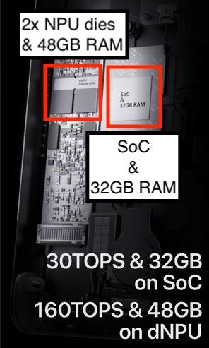
Here’s what I think the architecture actually looks like:
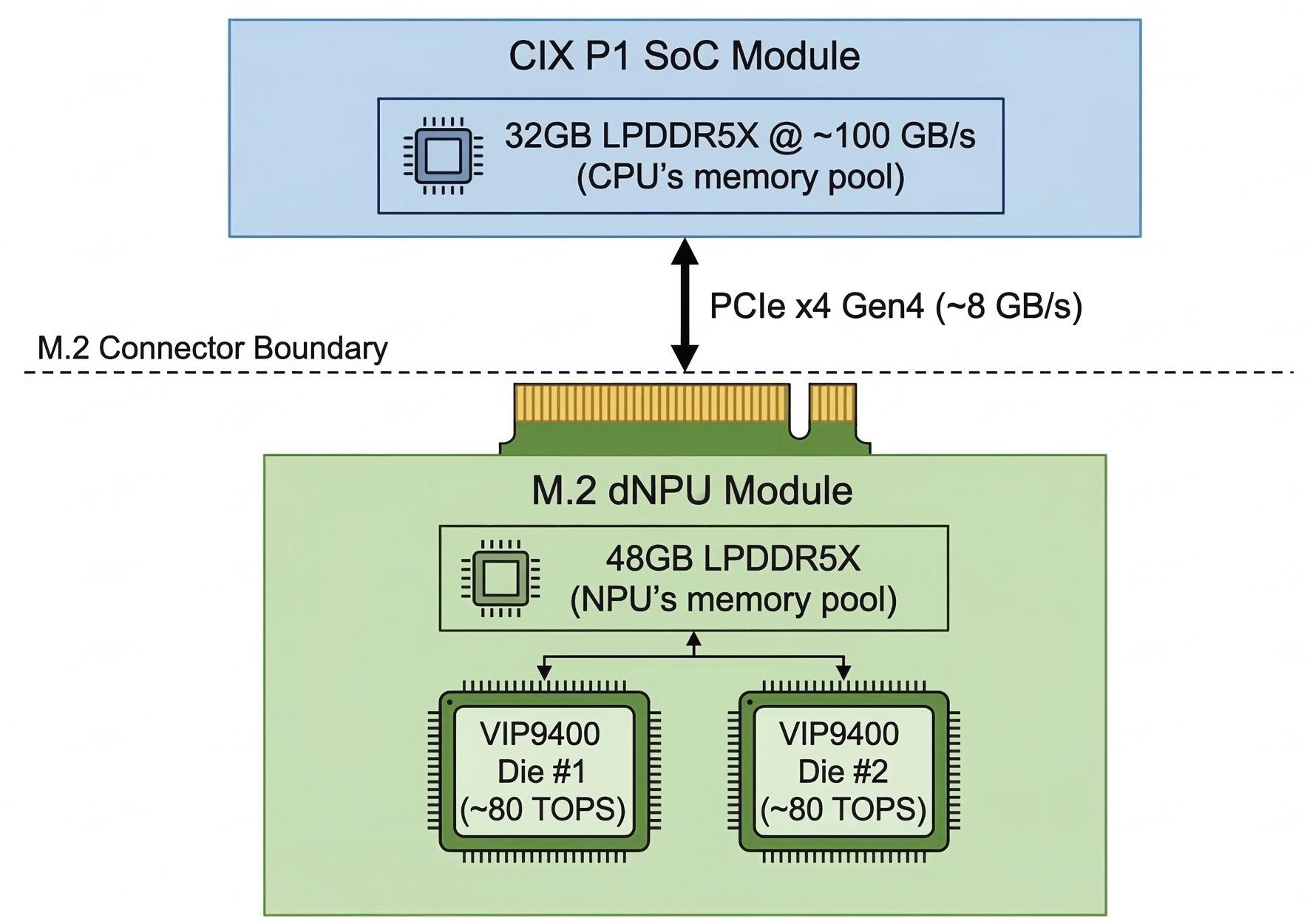
Both memory pools use LPDDR5X at 6500 MT/s, the CIX P1’s with a 128-bit bus that yields roughly 104 GB/s. We don’t know the dNPU’s memory bus width, but if it’s similar, both pools run in the ~100 GB/s range. But here is the catch, the dNPU sits on that M.2 card I already mentioned plugged into the SoC’s PCIe Gen4 x4 bus. That M.2 slot is the only data path between the two halves of this device and it is slow, 8 GB/s theoretical, ~6-7 GB/s effective.
TiinyAI quotes one bandwidth number because acknowledging two pools would require explaining the 8 GB/s straw between them, roughly a 12:1 bottleneck between each pool’s local bandwidth and the interconnect.
Why This Kills Inference Performance
LLM inference is memory-bandwidth bound. For each token generated, the active model weights must be read from memory. The speed at which you read weights determines your maximum token generation rate.
Each pool delivers strong bandwidth locally, but only for layers that live entirely within that pool. Any model spanning both pools has activations shuttling through the M.2 PCIe bus at 8 GB/s. The “160 TOPS” becomes a theoretical peak that will never be sustained when the model doesn’t fit entirely in the dNPU’s 48GB, which a 120B model at INT4 (~60GB total weights) cannot.
This isn’t a unified memory architecture like Apple Silicon, where CPU, GPU, and Neural Engine share one pool at 800+ GB/s, or even the DGX Spark, where the GB10’s 128GB is unified at 273 GB/s, and I already called that too slow. This is two separate compute units connected by a drinking straw.
Let’s Be Generous
Assume I’m wrong about PCIe Gen4 x4. Say the M.2 slot is Gen5 x4 (the CIX P1 doesn’t support Gen5, but humor me). That doubles the bus to ~16 GB/s. Still a fraction of either pool’s local bandwidth. PCIe Gen4 x8? The CIX P1’s M.2 slot is specced at x4, but even at x8 that’s ~16 GB/s. Same story.
The M.2 bus is the ceiling, no software optimization changes the bus width, this is the same lesson I learned with the DGX Spark: memory bandwidth is physics, not firmware.
“But PowerInfer Avoids Cross-Bus Transfers”
TiinyAI will argue that their PowerInfer implementation avoids shuttling full model weights across the PCIe bus, that’s why lean on it hard to every single website, page, video or press release you look at. The concept is relatively simple to understand, hot neurons compute on one side, cold neurons on the other, each side working only with weights already in its local memory.
Even accepting this framing, and as we’ll see, there are strong reasons to believe PowerInfer’s hot/cold classification doesn’t meaningfully apply to the MoE models, the results still have to be merged. Hot neuron outputs and cold neuron outputs must combine to produce the final activation for each layer. Whichever side performs the merge, the other side’s partial results must cross the PCIe bus, every layer, every token, at 8 GB/s. The activation tensors may be smaller than full weight matrices, but they’re not zero, and the latency compounds across dozens of layers and thousands of tokens during prefill.
The Bottleneck Is Worse Than Memory
Here’s what initially confused me, before I thought about the PCIe bus as a bottleneck the numbers were already too bad to be explained by memory bandwidth alone.
Look at it from the purely compute side, the dNPU claims 160 TOPS at INT8. For GPT-OSS-120B with 5.1B active parameters, each token requires roughly 10.2 billion operations. At 160 TOPS, the theoretical compute ceiling is approximately 15,600 tokens per second. Even at a poor 5% utilization, that’s 780 tok/s and they’re getting, based on KOL videos, 16.85 tok/s maximum. That’s roughly 0.1% utilization.
The DGX Spark comparison confirms it. The Spark uses the same class of memory LPDDR5X at roughly 2-3x the bandwidth. On comparable MoE models at 64K context, the Spark delivers 15-20 tok/s with fast prefill. The Pocket Lab delivers 4.47 tok/s with a 28-minute TTFT as you will see later. If the bottleneck were purely memory bandwidth, the gap would be 2-3x. Instead, the prefill gap is 100x+. The generation gap is 3-4x. Something in the ARM → NPU → dNPU coordination pipeline is burning almost all of the theoretical performance: synchronization overhead, clock domain crossings, data shuffling between three separate execution units that don’t share memory. They’re not compute-bound, or memory-bound, they’re architecture-bound.
Layer Sharding: Not a Feature, Not PowerInfer
PowerInfer’s layer sharding, splitting model layers across separate compute units, isn’t an optional optimization on this device. It’s a structural requirement. The model must be split across the two memory pools, and the split must be hand-tuned to minimize cross-pool transfers.
But PowerInfer’s core innovation, the hot/cold neuron classification, was designed for dense models. You profile which neurons fire frequently, preload “hot” neurons onto the GPU, and leave “cold” neurons on the CPU. The profiling works because dense model activations are predictable enough to classify in advance.
MoE models already have their own sparsity mechanism, the expert router decides at runtime which experts to activate for each token. Trying to layer PowerInfer’s neuron-level sparsity on top of MoE’s expert-level sparsity adds prediction overhead for minimal benefit, because the routing already determines which parameters are active. PowerInfer on MoE is redundant at best.
What TiinyAI almost certainly does is straightforward layer sharding: slice the model’s transformer layers, load some on the SoC’s 32GB pool and the rest on the dNPU’s 48GB pool, shuttle activations across the M.2 PCIe bus at each layer boundary. That’s not PowerInfer’s innovation. That’s basic model parallelism, the same thing llama.cpp does with --tensor-split. Every serious inference framework supports this, it’s the only option when your memory is physically split.
The GGUF Filename That Proves It
I came across an earlier version of TiinyAI’s desktop app, it showed a model selector with a revealing filename: gpt_oss_120b_layer_27_36.q4_0_4x64.gguf.
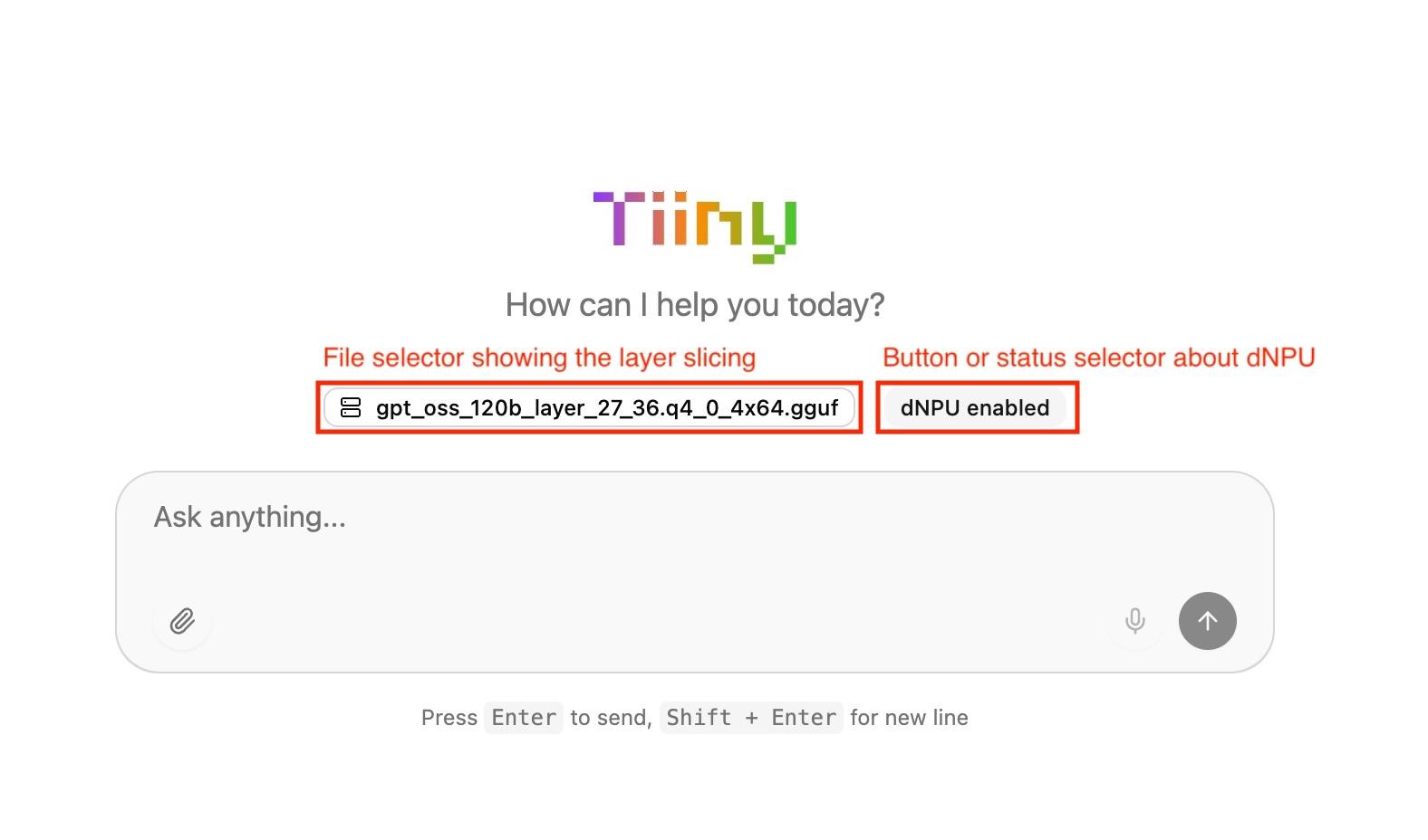
Read that filename. layer_27_36. That’s not dynamic hot neuron routing, that’s static layer assignment. Layers 27 through 36 are carved into a separate GGUF shard, almost certainly destined for one compute unit while the remaining layers run on the other. The sharding decision is baked into the file at conversion time, not computed at runtime like the market makes you believe.
The same screenshot shows a UI element reading “dNPU enabled,” either a toggle or a status indicator. If it’s a toggle, the implications are clear, you can disable the dNPU entirely, meaning the device has a fallback path to ARM-only execution, meaning the dNPU is a software-addressable peripheral on the PCIe bus, not an integrated part of the compute pipeline. It’s bolted on, not integrated. If it’s merely a status indicator, it still confirms the dNPU is a discrete component whose presence the system needs to explicitly acknowledge, not a seamless part of a unified architecture.
Every forward pass through a model spanning both compute units crosses the M.2 PCIe bus multiple times, not once per token, but once per layer-chunk boundary. If layers 0-26 run on the SoC’s NPU, layers 27-36 run on the dNPU, and layers 37+ return to the SoC, that’s two bus crossings per forward pass. At 8 GB/s with activation tensors in flight, the latency compounds with every token. This is why TTFT reaches 28 minutes at 64K context. Prefill has to process every input token through this layer ping pong, and the bus crossing overhead multiplies across thousands of tokens.
PowerInfer is the research paper that gets cited in press releases and probably investors. Static layer sharding across a PCIe bus is the engineering reality. They dress one up as the other because “we split model layers across two chips connected by a slow bus” doesn’t raise $1.7 million on Kickstarter or the seed round..
Not a Supercomputer, a Peripheral
The device isn’t standalone. It’s a USB-C peripheral. Every photo and video shows two cables: USB-C to the host computer (data), and a separate power connection (wall adapter or power bank).
The architecture is confirmed by TiinyAI’s own developer documentation at dev.tiiny.ai. The device exposes a virtual network interface over USB (a virtual NIC) and runs Linux on the ARM SoC:
device = TiinyDevice(device_ip="fd80:7:7:7::1")
api_key = device.get_api_key(master_password="your_password")
client = OpenAI(api_key=api_key, base_url=device.get_url())
The device gets a link-local IPv6 address, serves an OpenAI-compatible API endpoint, and the host computer connects over the virtual NIC. Different services like chat or Stable Diffusion run on different ports. A CLI tool called tiiny allows running models and benchmarks from the terminal.
One promotional video claims SSH access and Docker container deployment: “SSH into your system, deploy Docker containers, and run custom Python environments without any walled gardens or restrictions.” However, none of the KOL videos demonstrated this, and the developer documentation doesn’t mention SSH or Docker functionality. It’s a marketing claim without visible evidence but judging by the different port numbers I’ve seen it is likely that apps are docker containers.
The host computer runs TiinyAI’s desktop app (“TiinyOS”), which provides the chat UI, manages model selection, and handles downloads from TiinyAI’s model store. Model switching requires the desktop app or the cli tool.
To their credit: CES booth footage confirms the demo laptops were not connected to WiFi, with no cables other than USB going to the devices. The inference does appear to happen locally.
The device reportedly includes WiFi, Bluetooth, a microphone, and a speaker. The mic and speaker will allegedly be enabled via future OTA updates, these are likely targeting future speech models. Having said that a potentially always-on microphone on a USB device running closed-source software that phones home to download models is worth thinking about, especially given the corporate opacity we’ll examine later. The WiFi could theoretically enable standalone operation, but no KOL video demonstrated it.
So the “pocket supercomputer” is, architecturally, a Linux SBC with an NPU accelerator card, serving an OpenAI-compatible API over a USB virtual network link. The host provides the UI and internet connectivity. The device provides compute (slowly) and model storage (a 1TB NVMe SSD with that “bank-grade” AES-256 encryption that came free with the drive). For $1,399, you get a USB peripheral that needs your laptop to function, is locked to a proprietary model store, and delivers 12 tok/s at the context lengths its own marketing targets.
Model Lock-In: Architecture All the Way Down
As I said before, the “Tiiny format” conversion isn’t just NPU compilation through ACUITY; it’s also determining the static layer placement across two asymmetric memory pools. Which layers go on each side? How do you minimize M.2 bus crossings per forward pass? These sharding decisions are baked into the GGUF shard files at conversion time, as the layer_27_36 filename shows. That’s why you can’t download a GGUF from Hugging Face and run it.
This isn’t DRM. It’s architecture. The effect is identical: vendor lock-in dressed as ecosystem curation.
Part 4: The KOL Videos - What the Numbers Actually Show
I never got my hands on a Pocket Lab test unit, nobody outside TiinyAI’s chosen circle has. But approximately 4-5 days before the Kickstarter launch, KOL (Key Opinion Leader) review videos appeared on YouTube. These are influencer reviews, sponsored, seeded, or at minimum facilitated by TiinyAI. They are not independent technical evaluations.
The channel selection is telling. TiinyAI didn’t send units to any major tech reviewer. Nobody with millions of subscribers, nobody who does hardware teardowns, nobody who would ask “what SoC is this?” The channels that got early access were in the 48K-80K subscriber range. One reviewer spent more time excited about “uncensored models” than asking about architecture. Another channel (354K subscribers) isn’t even a tech review channel, it’s an SEO and backlinks channel. That “review” is someone reading TiinyAI’s script over their own slide deck and rendered demos, it’s not a review, it’s a paid commercial with someone else’s face on it.
Here’s the thing, if you built this device and it actually hit the numbers you claimed, you would send units to every tech reviewer on the planet and say “write whatever you want.” No review approval, no script, no restrictions. Apple sends review units to people who might trash them. NVIDIA lets AnandTech benchmark their GPUs against AMD. Confident companies invite scrutiny because independent validation is the most powerful marketing there is, and it’s free.
TiinyAI did the opposite. That tells you what unsupervised testing would reveal.
I watched them anyway, paused, timed, counted tokens, looked at every visible data point from the screen and it was shocking. It also confirmed my suspicions.
The Models: Almost All MoE
Nearly every model demonstrated is a Mixture of Experts architecture. The active parameters per forward pass, the number that actually determines inference workload, are a fraction of the headline count:
| Model | Total Params | Active Params | Architecture |
|---|---|---|---|
| GPT-OSS-120B | 117B | 5.1B | MoE |
| Qwen3-Coder-Next | 80B | 3B | MoE |
| GLM-4.7-Flash | 30B | ~3B | MoE |
| Qwen3-30B-A3B | 30B | 3B | MoE |
| GPT-OSS-20B | 21B | 3.6B | MoE |
| Qwen3-8B | 8B | 8B | Dense |
One reviewer did run Qwen3-8B, a dense 8B model, the only non-MoE model in any KOL footage. At 8B INT4, that’s about 4GB of weights which any modern phone can run. It’s not what justifies a $1,399 device.
The headline mode you see everywhere, GPT-OSS-120B, activates only 5.1B parameters per token which equates roughly to a compute workload of a 5B dense model. The other MoE models activate fewer parameters. The total weights still need to live in memory, a 30B MoE at INT4 is ~15GB, which is why the 80GB matters for loading. But the work the device does per token is 3-5B territory, not 120B territory but that is conveniently left out.
The Benchmark Conditions: Designed for Headlines
The visible benchmarks use 32 token output, roughly one short sentence, with context sizes starting at 256 tokens, about a paragraph. The prompts constrain the output to exactly 32 tokens with no reasoning or analysis. These are synthetic conditions engineered to produce optimal numbers, not anything resembling real usage.
The Speed Cliff: GPT-OSS-120B Decoding Performance
From the KOL benchmark footage:
| Context Length | Output Tokens | Decoding Speed |
|---|---|---|
| 256 | 32 | 16.85 tok/s |
| 512 | 32 | 16.77 tok/s |
| 1,024 | 32 | 16.43 tok/s |
| 2,048 | 32 | 15.38 tok/s |
| 4,096 | 32 | 14.42 tok/s |
| 8,192 | 32 | 12.04 tok/s |
| 16,384 | 32 | 9.16 tok/s |
| 32,768 | 32 | 6.04 tok/s |
| 65,536 | 32 | 4.47 tok/s |
Their best case, 256 token context, 32 token output, a 5.1B active-parameter model tops out at 16.85 tok/s, definitely a stretch to call this 20 tok/s performance and that’s their best number under synthetic conditions designed to maximize it.
But think about it, at short contexts, model weights and KV cache most of the time fit in one of the memory pools. As context grows, the KV cache expands, spills across pools, and every token generation starts hitting the 8 GB/s M.2 PCIe wall. The shape of the performance cliff in this table is the PCIe bottleneck made visible.
At 8K context, the minimum viable range for document Q&A, RAG, or coding assistance, you’re at 12 tok/s, at 32K, 6 tok/s and at 64K, 4.47 tok/s.
Live generation demos with small to medium context size showed approximately 14 tok/s, consistent with the table data.
The TTFT Disaster
Another frame of a KOL video showed the TTFT or time to first token benchmark data and I was laughing at this point.
| Model | TTFT @ 256 ctx | TTFT @ 8K ctx | TTFT @ 64K ctx |
|---|---|---|---|
| GPT-OSS-120B | ~5.3s | ~75s | ~1,706s (28 min) |
| Qwen3-30B-A3B | ~26s | ~19s | ~97s |
| GPT-OSS-20B | ~1.8s | ~7.5s | ~53s |
Twenty-eight minutes to first token on GPT-OSS-120B at 64K context. On a model that only activates 5.1B parameters per token on a device marketed for “always-on AI agent workflows.” Half an hour of staring at a blank screen before the “supercomputer” produces its first word.
Even Qwen3-30B-A3B, 3B active parameters, hits 97-second TTFT at 64K context. Think about what that means for the coding and agent workflows TiinyAI markets. You load a few source files, make some tool calls, accumulate conversation history, and suddenly you’re at 32K-64K context. Every iteration, every “fix this bug,” every “run the tests,” starts with a minute-plus wait before the first token. Modern agentic coding is a tight loop: read, change, test, adjust, when each cycle starts with a 90-second stare at a loading spinner, that loop doesn’t slow down, it becomes unusable.
The “12.4 tok/s Average” and the KOL Who Outed Himself
One reviewer said the quiet part out loud, showing the benchmark table on screen, he told viewers: the numbers at the bottom are skewed lower because they go up to 65,000 tokens, which isn’t typical for average applications, so the real-world test is probably the first half of the table, and those speeds are “broadly in line” with the marketing material.
The “first half of the table” is 256 to 2,048 tokens, roughly one to four pages. This reviewer is telling his audience that “typical use” means asking an LLM questions about a few paragraphs of text. Meanwhile, TiinyAI’s own marketing lists RAG and document Q&A, coding copilots, and agent workflows with multi-turn reasoning at 8K-32K context. Companies are shipping models with 128K-1M context windows because real utility demands it. Summarizing a PDF needs 8K-32K minimum, a coding assistant needs 8K-32K easily and an agent workflow with tool calls needs 16K-64K+.
At TiinyAI’s own stated use cases:
| Context | Decoding Speed | Use Case |
|---|---|---|
| 8,192 | 12.04 tok/s | Minimum for RAG/document Q&A |
| 16,384 | 9.16 tok/s | Coding with files loaded |
| 32,768 | 6.04 tok/s | Agent workflows |
That’s 6-12 tok/s, not 20 like they love to claim everywhere.
Also I noticed that the reported “12.4 tok/s average” is inflated because the benchmark oversamples tiny context sizes that are too short for any use case that TiinyAI actually markets. Filter it to 4K+ context and you get an average of 9.23 tok/s, if you filter to 8K+ context size you get an average of 7.93 tok/s.
The Coding Demo Reality
One reviewer used GLM-4.7-Flash, 3B active parameters, with an agentic coding tool. The request was to make a simple 3D flight game. Prefill was fast-forwarded, a common pattern across all KOL footage, where loading, thinking, and prefill times are consistently edited out via jump cuts. Chain-of-thought took 30+ seconds per iteration, the first prompt went in at 1:48 AM based on the logs and coding finished at 2:00 AM. Twelve minutes, approximately 20K tokens in context, producing 23 lines of HTML, 46 lines of CSS, and 249 lines of JavaScript.
The result: a “3D flight game” with no physics engine. The plane floats static in space until you press W to move forward, no thrust, no gravity, no momentum. Twenty minutes of inference for a WASD-controlled floating box, the reviewer acknowledged the time but offered: “it’s not about the speed, it’s about the result and the fact that we could do it.”
Another reviewer explicitly stated: “I won’t be giving the model massive walls of text or insanely difficult tasks.” Translation: I’m going to use tiny contexts so the numbers look good. His GPT-OSS-120B test showed 14 tok/s.
Every coding test across all videos was simple HTML, CSS, and JavaScript, single-file toy apps. Nobody threw a real codebase at it, nobody tested with 50K tokens of Python because at those context sizes, the device would choke and everyone involved seems to know it.
Model Lock-In Confirmed
Multiple reviewers confirmed you cannot download models from Hugging Face and run them directly. You’re limited to TiinyAI’s model store. One stated explicitly that these models “have been optimized to run at high speed on the Tiiny AI pocket computer,” which is the ACUITY/NBG compilation requirement manifesting as product policy. The VIP9400 NPU can’t run arbitrary model formats. Every model must be pre-compiled for their specific hardware configuration.
For Perspective
A consumer NVIDIA RTX 4060 Ti, a $400 graphics card, can run Qwen3.5-35B-A3B, a comparable 3B active-parameter MoE model, at over 80 tok/s on a single sequence with 100K+ context. That’s roughly 7x faster, with dramatically more context headroom, at less than a third of the price.
Part 5: The “120B” Misdirection
I’ve already touched on this a bit, TiinyAI’s headline claim: “Runs GPT-OSS-120B (INT4) locally at 20 tokens per second.” Or simply “120b models”. For someone reading this it’s hard not to convey they mean dense.
A dense 120B model at INT4 requires reading ~60GB of weights per token. At 100 GB/s memory bandwidth, that’s a theoretical maximum of 1.7 tokens per second, that’s very far from the advertised magic 20 Tok/s.
GPT-OSS-120B is a Mixture of Experts model. OpenAI’s own documentation states it plainly: “117B parameters with 5.1B active parameters.” At INT4, that’s ~2.55GB of weight reads per token. At 100 GB/s: ~39 tok/s theoretical. Now 20 tok/s makes sense, because the device is doing the work of a 5B model, not a 120B model.
They chose GPT-OSS-120B specifically because its total parameter count sounds impressive while its active parameter count is small enough for their hardware. Every piece of marketing says “120B.” Not once do they say “5.1B active.” Not once do they say “Mixture of Experts.” Not once do they explain that the per-token workload is 24x smaller than the headline number implies. The omission is consistent, systematic, and deliberate.
Part 6: The Research - PowerInfer and TurboSparse
Back in Part 2, I mentioned that TiinyAI’s software stack is built on PowerInfer, and that they didn’t write it or did they? Before we examine what TiinyAI claims about this research, we need to understand what the research actually is and who actually created it.
PowerInfer (December 2023)
PowerInfer is a research project from the Institute of Parallel and Distributed Systems (IPADS) at Shanghai Jiao Tong University (SJTU). The paper was published on arXiv on December 16, 2023, by Yixin Song, Zeyu Mi, Haotong Xie, and Haibo Chen. It was accepted at SOSP 2024, one of the most prestigious systems conferences in the world, with a 17.3% acceptance rate.
The key insight is genuinely clever. LLM inference exhibits a power-law distribution in neuron activation. A small subset of “hot” neurons fire consistently across all inputs. The majority of “cold” neurons only activate for specific inputs. PowerInfer exploits this by preloading hot neurons onto the GPU and computing cold neurons on the CPU, dramatically reducing GPU memory requirements and data transfers. The paper demonstrated up to 11.69x speedup over llama.cpp on consumer hardware.
Critically, PowerInfer was designed for and evaluated exclusively on dense models: OPT-175B, LLaMA2-70B, Falcon-40B. The hot/cold profiling assumes dense activation patterns where individual neurons have stable, predictable firing rates. MoE architectures barely existed in open-source when the paper was submitted (Mixtral 8x7B dropped days before PowerInfer’s arXiv date). The paper makes no claims about MoE models. Remember this.
TurboSparse (June 2024)
The follow-up from the same SJTU IPADS team introduced TurboSparse, a technique for making models more sparse by retraining them so that fewer neurons fire during each forward pass. Unlike PowerInfer’s runtime optimization, TurboSparse modifies the model itself and was applied to both dense models (Mistral) and MoE models (Mixtral). For TurboSparse-Mixtral-47B, active parameters drop to about 4B per forward pass.
The distinction matters: PowerInfer is a runtime inference trick that only works on dense models. TurboSparse is a model modification that works on both. TiinyAI markets them as a single package (“our proprietary technologies, TurboSparse and PowerInfer”), but they solve different problems, apply to different architectures, and the one TiinyAI leans on hardest (PowerInfer’s “hot neuron” narrative) is the one that doesn’t apply to the MoE models they actually run.
PowerInfer-2 (June 2024)
PowerInfer-2 extended the framework to smartphones. The key result, 11.68 tokens per second running TurboSparse-Mixtral-47B on a phone, depended on TurboSparse’s modified model weights. Without TurboSparse, the stock Mixtral model wouldn’t hit those speeds. Same SJTU IPADS team.
This is real, peer-reviewed science from a respected university lab. The research is genuinely impressive. But notice what all three projects have in common: they were developed at SJTU, published under SJTU affiliation, and authored by SJTU researchers. The question is not whether PowerInfer works. The question is who owns it and who’s selling it.
Part 7: The Research Attribution
The Timeline That Doesn’t Add Up
TiinyAI’s Kickstarter page includes a timeline graphic:
- Jan 2024: Team founded
- Jun 2024: Launched the open-source projects PowerInfer and TurboSparse
- Apr 2025: Introduced Tiiny AI Pocket Lab prototype
- Nov 2025: Entered pilot production
- Dec 2025: Set Guinness World Record
- Jan 2026: Showcased at CES
- Mar 2026: Kickstarter live
- May 2026: Mass production
- Aug 2026: Start shipping
Read line two again: “Jun 2024 - Launched the open-source projects PowerInfer and TurboSparse.”
PowerInfer was published on arXiv on December 16, 2023, a month before TiinyAI’s “team founded” date. The research predates the company. The paper was submitted, peer-reviewed, and published under Shanghai Jiao Tong University’s institutional affiliation, funded by university resources, using university infrastructure.
TiinyAI didn’t “launch” PowerInfer. SJTU researchers published it. TiinyAI forked it.
The Fork
TiinyAI’s GitHub is github.com/Tiiny-AI/PowerInfer, originally a fork of github.com/SJTU-IPADS/PowerInfer. The product announcement sits directly in the forked README. The original research code, published by academics at a public university, is the foundation of a commercial product sold to 1,266 backers for $1.7 million.
Update: Since this post was drafted, the original SJTU-IPADS/PowerInfer repository now redirects to Tiiny-AI/PowerInfer. The commit history is still there, but the SJTU IPADS URL is gone. Anyone searching for the original academic project lands on TiinyAI’s repo instead.
TiinyAI’s PR Newswire press release describes PowerInfer and TurboSparse as “Tiiny AI’s proprietary optimization technologies.” Proprietary. The code is on a public GitHub repository under an open-source license.
Looking at the GitHub contributors tells its own story. The accounts with recent commits are almost entirely empty profiles: AliceRayLu has a handful of repos and a burst of contributions around April 2025. ZeyuMi has zero public repos. wisman-tccr is another empty account. The one profile with actual information is jeremyyx, whose GitHub bio lists SJTU as affiliation, Shanghai as location, and links to yixinsong-e.github.io, Hugging Face, and a Google Scholar profile. That’s Yixin Song, the first author on the original PowerInfer paper.
So the connection between SJTU IPADS and TiinyAI isn’t just a fork. At least one of the original paper authors is actively committing code. The question becomes: did the SJTU researchers start TiinyAI, or did TiinyAI recruit them? Either way, the Kickstarter timeline claiming “Jan 2024: Team founded” followed by “Jun 2024: Launched the open-source projects PowerInfer and TurboSparse” is misleading. PowerInfer was published in December 2023 under SJTU’s name, a month before TiinyAI supposedly existed. And now the academic repo redirects to the commercial one. The commit history is preserved, but the URL isn’t. Anyone looking for the SJTU IPADS research finds TiinyAI’s brand instead.
Part 8: The Corporate Opacity
Where Is the CEO?
When you build the world’s smallest AI supercomputer, verified by Guinness, and you’re the CEO, your name is everywhere. Tim Cook demos the iPhone. Jensen Huang demos everything in a leather jacket. If you’ve cracked pocket-scale 120B inference, you are printing credibility.
And beyond the business logic, think about the ego. Tech startup founders are not known for their humility. If you just cracked what should be physically impossible, running 120B models at 20 tok/s in a pocket device, your name would be plastered across every platform. Even if TiinyAI fails, being known as “the person who built the pocket AI supercomputer” prints money for the rest of your career. Every VC takes your next meeting. Every job offer starts at C-suite.
No tech founder in history has cracked a problem this visible and then hidden behind a GTM Director.
TiinyAI has no named CEO, no named CTO, no named chief scientist and no named founder.
The only visible person is Samar Bhoj, “GTM Director.” A marketing role. He was the face at CES 2026. In press photos, he holds the device. In press releases, he’s quoted.
The LinkedIn Census
I searched LinkedIn for “Tiiny AI.” The entire visible workforce is four profiles.
Profile 1: “LinkedIn Member” - Vice President at Tiiny AI Inc. Based in Dover, Delaware. Profile locked. Name hidden. Reverse image search: nothing. The VP of the hottest AI hardware startup in America is a ghost.
Profile 2: Satyendra B - GTM Director at Tiiny AI Inc. Also Dover, Delaware. No profile photo. No prior work experience. Only LinkedIn interests: ARM, Perplexity, OpenAI, Samsung, AMD, NVIDIA, GitHub. 35 connections. 10 posts total, all about TiinyAI, the oldest roughly one month old.
Here’s the thing though. TiinyAI’s PR Newswire press releases all quote “Samar Bhoj, GTM Director.” Not Satyendra B. Same title, same company, same location, different name. The “B” could stand for Bhoj, making these the same person. Or these could be two different people sharing the same title, unusual for a four-person company. Or one of the names is fabricated. The single most visible human in the entire organization can’t maintain a consistent identity across platforms.
Profile 3: Rosa Dai - Investment Manager at Gobi Partners. Based in Hong Kong. Her profile lists TiinyAI as a portfolio company alongside Liko.ai, Zenowell, and Lymow Medtech.
Profile 4: “LinkedIn Member” - Profile locked. Hong Kong. Current role translates from Chinese as “实习学生 at tiiny ai,” meaning “Intern at Tiiny AI.” Pixel art avatar.
That’s it. Four profiles: a hidden VP, a GTM director with no career history, a Hong Kong VC analyst, and a Hong Kong intern. Zero engineers, zero researchers, zero of the MIT/Stanford/Meta alumni, zero of the SJTU IPADS authors whose papers power the product.
Engineers who worked at Meta have LinkedIn profiles and so do engineers who worked at Intel. Stanford and MIT graduates have LinkedIn profiles, if they joined a company breaking Guinness records and raising millions, their profiles would list TiinyAI as their current employer. Either these people don’t exist, or they don’t want to be found.
The Gobi Partners Connection
Rosa Dai works at Gobi Partners, a pan-Asian VC firm headquartered in Hong Kong and Kuala Lumpur with $1.7 billion AUM. Gobi Partners runs the Gobi-Redbird Innovation Fund, specifically designed to commercialize HKUST research. The fund’s press release explicitly names Lymow, the same Lymow in Rosa Dai’s portfolio alongside TiinyAI.
TiinyAI claims team members from HKUST. Gobi Partners has a dedicated fund for HKUST research commercialization. Gobi’s analyst lists TiinyAI as a portfolio investment, the “multi-million dollar seed round from leading global investors” that Crunchbase won’t name almost certainly came through Gobi Partners’ HKUST pipeline.
This isn’t a Silicon Valley startup that happened to take Asian money,this is an HKUST/SJTU research commercialization project, funded through a Hong Kong VC’s university pipeline, packaged in a Delaware LLC for US market access.
The GitHub Ghost Town
The Tiiny-AI GitHub organization has one repository: the PowerInfer fork. The last commit was two months ago, a README.md edit to add the product announcement. No other repositories, no SDKs, no tools, no documentation repos.
The person who made that commit has zero public repositories and zero visible commit history.
Compare this to any real AI startup with MIT/Stanford/Meta-caliber engineers. Their GitHub organizations have dozens of repos, their contributors have years of commit history. TiinyAI’s GitHub has the surface area of a placeholder.
Meanwhile, a Shenzhen-based GitHub user (DIPTE) maintains a curated “awesome-stars” repository among the starred repos: VeriSilicon/TIM-VX and Tiiny-AI/PowerInfer. Someone in Shenzhen is tracking both VeriSilicon’s NPU software and TiinyAI’s inference engine. Circumstantial, but consistent with everything else.
The Question
The device appears to work. KOLs used it, CES attendees interacted with it, tokens appeared on screen. I’m not claiming this is vaporware, but if your marketing claims are real, if you’ve genuinely built the world’s smallest AI supercomputer, where is the CEO? Where is the CTO?
In the middle of the AI revolution, can you imagine inventing a pocket device that runs 120B models and not wanting your name on it? Not wanting to be on LinkedIn, TechCrunch, CNBC, every conference stage?
Yet TiinyAI has a hidden VP, a GTM director with no career history, a VC analyst in Hong Kong, and an intern in Hong Kong. That’s it.
The absence of visible leadership isn’t a gap. It’s the architecture.
Just Call It What It Is
Every piece of evidence points in one direction. The hardware uses Chinese silicon (CIX P1 from Shenzhen, VIP9400 from Shanghai), the research comes from a Chinese university (SJTU in Shanghai), the PR distribution runs through Hong Kong, the Guinness record was established in Hong Kong, the seed investor operates from Hong Kong and two of the four LinkedIn employees are in Hong Kong.
And yet: every press release calls TiinyAI “a U.S. AI Infra startup.” The Kickstarter displays “Dover, Del.” The GTM Director presents it as an American product.
There’s nothing wrong with being a Chinese company selling hardware in the US market. Plenty of excellent hardware comes from China. But if that’s what you are, say so. Don’t incorporate a Delaware shell, hire an English-speaking GTM Director as the face, stamp “US startup” on every press release, and hope nobody notices that every operational thread traces back to Shanghai, Shenzhen, and Hong Kong. That’s not localization, that’s misrepresentation and 1,266 Kickstarter backers deserve to know who they’re actually buying from.
Part 9: The VeriSilicon Theory
I want to be explicit: what follows is informed speculation, not proven fact. But the circumstantial evidence is substantial enough that someone should be asking these questions.
The Evidence Chain
- The dNPU is almost certainly VeriSilicon VIP9400 dual-die (80 TOPS × 2 = 160 TOPS)
- VeriSilicon is Shanghai-based (688521.SH, publicly traded)
- VeriSilicon builds custom boards and NPU modules as a core competency
- VeriSilicon’s entire business model is SiPaaS (Silicon Platform as a Service). A multi-million dollar seed round is exactly the budget for a SiPaaS engagement
- VeriSilicon launched the Coral NPU IP jointly with Google in November 2025, demonstrating end-to-end capability from IP design to commercial hardware
- VeriSilicon’s June 2025 press release announced their NPU IP “now supports on-device inference of large language models,” actively marketing LLM inference capability at exactly the time TiinyAI was building the Pocket Lab
- TiinyAI’s boards are custom-built (off-the-shelf boards don’t fit the form factor)
- Custom PCB design, enclosure tooling, injection molds: these require manufacturing capability a startup with a $10K Kickstarter goal doesn’t have
- TiinyAI’s press releases originate from Hong Kong, where VeriSilicon has operations
- The Guinness record was established through Hong Kong
- The SJTU IPADS connection is Shanghai, same city as VeriSilicon HQ
- A Shenzhen-based GitHub user stars both
VeriSilicon/TIM-VXandTiiny-AI/PowerInfer
What This Would Explain
If TiinyAI is a subsidiary or front for VeriSilicon, or a similar established Chinese semiconductor firm, every anomaly resolves: no CEO/CTO because leadership sits at the parent; Hong Kong distribution because that’s where the parent handles international operations; Delaware LLC as a US sales entity; no named investors because the “seed round” came from the parent; $10K Kickstarter goal because the real R&D budget comes from the parent; GTM Director as sole visible person because he’s literally the go-to-market face; custom boards because they have in-house manufacturing.
I cannot prove this. But the shape of what’s visible is consistent with deep VeriSilicon involvement.
Here’s the thing though, the split memory architecture actually argues against the subsidiary theory. If VeriSilicon created TiinyAI as a consumer brand, why split the memory? VeriSilicon owns the NPU IP, they own the fab relationships, they could design a single board with 80GB unified behind the VIP9400 and a lightweight ARM host for orchestration. No PCIe bottleneck, no layer sharding nightmare. A VeriSilicon spinoff would have done it right, because they could.
The split memory looks more like the decision of a team that couldn’t put it all on one board. Budget constraints, timeline pressure, lack of control over the silicon design. That points to an independent team, possibly connected to the SJTU/HKUST research network, funded through Gobi Partners, who contracted VeriSilicon’s SiPaaS for the NPU module and paired it with an off-the-shelf CIX P1 because it was the fastest path to a prototype. They took the cheap path and accepted the architectural compromises. Then they hid those compromises behind “120B” headlines.
The early prototype photo supports this.
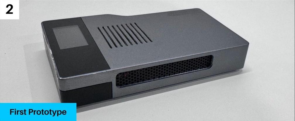
It shows what appears to be an off-the-shelf PCIe NPU card inside an enclosure, the kind of thing you’d build by taking a commodity SBC, connecting an NPU evaluation board via a PCIe-to-M.2 ribbon adapter, and writing enough software to demo it. The problem is what happened next: instead of redesigning for production, unifying the memory, eliminating the PCIe bottleneck, etc, they just miniaturized the prototype. Shrunk the card down to M.2 22110 format, added external LPDDR5X to the dNPU board, kept the same split-pool architecture, and put it in a fancy enclosure. The PCIe bottleneck isn’t a design tradeoff; it’s a prototype artifact they never fixed.
Either way, both theories end at the same conclusion: the marketing is systematically misleading regardless of who’s behind the company.
But the two theories might not be mutually exclusive. Theory A explains the architecture: a budget-constrained team that prototyped from off-the-shelf parts and miniaturized without redesigning. Theory B explains the corporate structure: the invisible leadership, the HK operations, the shell company.
The synthesis: a small research team connected to SJTU/HKUST built the prototype. A larger entity, possibly VeriSilicon, possibly another company with fab access, funded the productization through the seed round and provides manufacturing infrastructure. The Delaware LLC obscures the relationship, Gobi Partners provides the VC paperwork, the Kickstarter provides the cover story of a scrappy US startup.
The funding math supports this. The $1.7M Kickstarter doesn’t cover the real costs: SiPaaS NRE for the dNPU module, PCB tooling, injection molds, component costs at scale (80GB of LPDDR5X at pre-crunch pricing was $200-300 per unit, more now), FCC/CE certification, global logistics, and the software development. The “multi-million dollar seed round” predates the Kickstarter. Somebody already wrote the real check, the Kickstarter is demand validation and marketing, not funding.
And whoever wrote that check doesn’t want their name on this product. No CEO, no CTO, no named founder, no named investor. In the middle of the AI revolution, someone funded a hardware device that allegedly runs 120B models in your pocket, and every single person involved is hiding.
That’s not how legitimate startups work, that’s how you build something designed to be abandoned if things go wrong.
Part 10: The $10,000 Question
A hardware product with custom PCB design, 80GB of LPDDR5X RAM, a dual-die 160 TOPS NPU on an M.2 carrier, thermal management in a pocket form factor, FCC/CE certification, and a global logistics chain does not cost $10,000 to bring to production. The RAM alone would eat that for a handful of units.
A $10K goal on a hardware Kickstarter is a marketing stunt. It lets you claim “16,000% funded!” in press releases. Real hardware Kickstarters set goals that reflect actual production costs. TiinyAI set $10K because the headline was the product.
Estimated delivery: August 2026. Five months from a company that has never publicly shipped a consumer hardware product. Unless the manufacturing capability already exists elsewhere and the Kickstarter is just the storefront.
The Press Distribution Map
The PR Newswire press release carries distribution code HK08267, a Hong Kong wire release, syndicated globally to create the appearance of widespread media coverage:
Fidelity Investments (US financial news), Morningstar (US financial), Bangkok Post (Thailand), Manila Times (Philippines), Thailand Business News, Geo News (Pakistan), TechRadar (UK), Digital Trends (US), WCCFTech, Benzinga. All from a single Hong Kong press release. The Southeast Asian distribution isn’t random, PR Newswire Hong Kong radiates to English-language publications across the region automatically, every placement generates a Google News result, every result becomes social proof.
None of these outlets did original reporting, they reprinted a press release from Hong Kong and TiinyAI lists them as “Trusted by Top Media.”
The Pre-Written Exit
Kickstarter requires every project to write its own “Risks and Challenges” section, TiinyAI’s reads like it was copied from a crowdfunding playbook:
“Just like any crowdfunding journey, there are always a few risks along the way. Bringing an innovative new product through development and mass production can lead to unexpected surprises. However, thanks to our close work with long-term, trusted manufacturing partners, there is a solid foundation to navigate any hiccups smoothly.”
“Unexpected surprises.” “Trusted manufacturing partners.” “Navigate any hiccups smoothly.” This is a pre-written excuse. When LPDDR5X prices spike, or the dNPU yield is bad, or FCC certification takes longer than expected, the language is already in place.
Kickstarter’s own terms say they don’t guarantee projects or investigate creators’ ability to deliver. If the Delaware LLC dissolves, the money is gone. There’s nobody to sue: no named CEO, no named CTO, no named founder, no named investor. Just a GTM Director with an empty LinkedIn profile and an intern in Hong Kong.
What An Honest Product Page Would Say
I’m not saying the hardware can’t work, the CIX P1 is real, the VIP9400 is real, powerInfer works, MoE helps. All true. It’s possible this is a legitimate academic spinout from SJTU researchers who built something real but have terrible marketing instincts and no idea how to present a company to Western audiences. The GitHub evidence connecting Yixin Song to TiinyAI’s codebase supports this reading. Maybe they’re not hiding, maybe they just don’t know how to be visible.
But the pattern of omissions is too consistent to be accidental. They never say “MoE”,they never say “5.1B active”, they never say “split memory”, they never say “PCIe bottleneck”, they never name the SoC, they never name the NPU, they never name the CEO. Every single piece of information that would let a buyer make an informed decision is missing, and every single piece of information that sounds impressive is front and center. That’s not bad marketing, that’s good marketing in service of a misleading pitch.
Here’s the uncomfortable truth TiinyAI’s pitch dances around: there is no cheap off-the-shelf solution that gives you 160+ TOPS of NPU compute, 80GB+ of unified memory, and a portable form factor at consumer prices. That combination doesn’t exist in current silicon. Apple solved it by spending billions on custom unified memory architecture. NVIDIA solved it with HBM at datacenter prices. Nobody has solved it at the consumer price point TiinyAI targets.
So TiinyAI duct-taped a solution together: an ARM SoC with its own memory pool, a discrete NPU card with a separate memory pool, connected by a PCIe bus that’s 12x slower than either pool’s local bandwidth. It technically works. It performs poorly because the device is fighting its own architecture every step of the way.
And a unified pool was achievable at the same price point. The 80GB of LPDDR5X is already paid for; they just split it across two boards instead of putting most of it behind the dNPU with a wider memory controller. Leave the ARM SoC with 4-8GB to run Linux and orchestration, give the NPU 72-76GB of unified local memory, and the PCIe bottleneck disappears for any model that fits. Same components, same cost, radically better architecture. They didn’t choose the split because of budget; they chose it because they prototyped with off-the-shelf parts and never redesigned for production.
An honest listing would read:
“Portable USB AI inference accelerator. Runs MoE models with up to 120B total parameters (5.1B active per token) at 12-16 tokens per second on short-context benchmarks. Performance degrades significantly at longer contexts; expect 6-9 tok/s at 8K-32K, with TTFT reaching minutes at 32K+ context. Requires host computer with our desktop app. Split memory architecture (32GB SoC + 48GB dNPU) connected via PCIe Gen4 x4. Models limited to our pre-optimized store. Inference engine based on PowerInfer, developed at SJTU’s IPADS lab.”
That description, at $1,399, would be a hard sell, which is exactly why they don’t use it.
That’s a real product at a real price. It’s also exactly the kind of thing the open-source community was already exploring. A year before TiinyAI’s Kickstarter, someone posted on r/LocalLLaMA describing a DIY cluster with the same architecture: ARMv9.2 boards with 30 TOPS NPUs, 64GB RAM at 100 GB/s, NVMe storage, running distributed inference with llama.cpp. Same chip specs, same memory, same approach. The community was discussing this design openly and for free, TiinyAI put it in a fancy enclosure and raised millions for it.
I wanted it to be real. The physics didn’t care.
Neither did the math.
All hardware identification in this post was derived from TiinyAI’s own publicly shared marketing images, social media posts, exploded-view renders, prototype photos, spec sheets, press releases, and Kickstarter page. Additional sourcing includes academic papers, GitHub repositories, LinkedIn profiles, corporate registrations, and DNS records, all publicly accessible. No proprietary, leaked, or confidential information was used. No devices were obtained, tested, or disassembled. No NDAs were violated because none exist. They showed me everything I needed. I just looked.
I have no financial position in or relationship with TiinyAI, CIX Technology, VeriSilicon, Gobi Partners, or any entity mentioned in this post. I did not back the Kickstarter campaign.