Disclosure: English is my third language and I can’t write for shit in any of them. I used AI to help me write this post. The research, hardware identification, bandwidth math, OSINT, and conclusions are entirely mine. The AI helped me say it without making your eyes bleed. If you’d rather argue about prose than PCIe bottlenecks, this isn’t the post for you.
Update (March 24): TiinyAI Responded. I Did More Math. It Got Worse.
After this post went live, TiinyAI responded to backer questions on Kickstarter with some revealing technical details. I wanted to be fair, so I went back to the drawing board with their new information to see if my original analysis still held. If the data proved me wrong, I’d say so.
It didn’t prove me wrong. It made the picture worse.
What TiinyAI Said
In a private message to a backer (later shared publicly in the comments), TiinyAI confirmed the split memory:
The 80GB of memory is divided into two independent memory domains. The SoC side has about 102 GB/s of bandwidth, and the dNPU side has about 154 GB/s. Since they operate separately, they can be accessed at the same time, giving a combined bandwidth of around 240 to 250 GB/s.
In a follow-up, they directly addressed the PCIe bottleneck:
The system uses PCIe Gen4 x4 with a bandwidth limit of about 8 GB per second. This only matters during large data transfers such as loading a model into memory. During token generation, it only transfers small activation data needed to combine results. Using a model with hidden dimension 2880 and FP16 precision, the data transferred per step is about 5.6 KB. Transferring this over an 8 GB per second connection takes a tiny fraction of a millisecond. The bandwidth is more than sufficient.
They also claimed:
Computation is done in parallel across both rather than step by step.
And:
We can confirm the merging of hot NPU and cold SoC neurons is not limited by PCIe bandwidth.
I went back and tested all of it. Starting with the easy ones.
The “240–250 GB/s Combined Bandwidth” Claim
Calling the aggregate bandwidth of two isolated memory pools “combined 240–250 GB/s” is meaningless. Each pool serves its own local compute. The dNPU can’t read from the SoC’s 32GB at 154 GB/s. The SoC can’t read from the dNPU’s 48GB at 102 GB/s. The only path between them is the M.2 PCIe bus at 8 GB/s.
For context, the DGX Spark has 273 GB/s of actually unified bandwidth where every byte is accessible to every compute unit at full speed. I already called that too slow. TiinyAI wants you to compare their 250 against NVIDIA’s 273 and think they’re competitive. One number is real. The other is two garden hoses on opposite sides of a house.
The 5.6 KB Claim
Their math: hidden dimension 2880 × 2 bytes (FP16) = 5,760 bytes ≈ 5.6 KB per layer boundary crossing. For single-token decode, that’s correct and that’s small. At 8 GB/s it transfers in a fraction of a millisecond. They’re right that the raw data transfer speed isn’t the limiting factor for small payloads.
Which made me ask: if 8 GB/s bandwidth isn’t the bottleneck per se, then what is? Because the performance is still terrible and something has to explain it.
So I went back to the KOL benchmark footage frame by frame.
The Real Performance Ceiling: Memory Bandwidth, Not Compute
In the original post I framed the bottleneck in terms of TOPS utilization. That was wrong. LLM inference at this scale is memory-bandwidth-bound, not compute-bound. The relevant question isn’t “how many operations per second” — it’s “how fast can you read the active weights from memory per token.”
GPT-OSS-120B: 5.1B active params × 0.5 bytes (INT4) = 2.55 GB of weight reads per token.
If everything ran on the dNPU at 154 GB/s with no splitting:
2.55 GB ÷ 154 GB/s = 16.6 ms per token ≈ 60 tok/s ceiling.
If everything ran on the NPU at 102 GB/s:
2.55 GB ÷ 102 GB/s = 25 ms per token ≈ 40 tok/s ceiling.
Those are the theoretical bandwidth ceilings. No real system hits 100% — 50-60% is good utilization. So a well-implemented device running this model on the dNPU alone should deliver roughly 30-36 tok/s.
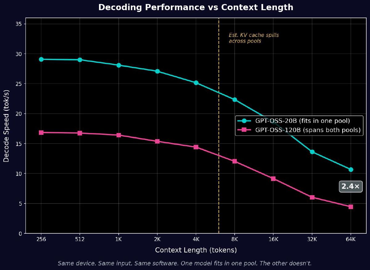
They get 16.85 at short context. About 28% of the bandwidth ceiling. And it gets much worse from there.
What the Benchmark Data Actually Shows
From the KOL benchmark screens for GPT-OSS-120B at 65K context:
Prefill: 1,698,543.6ms @ 10.6 tok/s
Decoding: 7,164.1ms @ 4.47 tok/s
Output: 140 chars, 32 tokens
Total: 1,706.001s
We can calculate the actual input size from the prefill data:
1,698,543.6 ms × 10.6 tok/s ÷ 1,000 = ~18,005 input tokens
Decode verification: 32 tokens ÷ 4.47 tok/s = 7,158 ms ≈ 7,164 ms ✓
The numbers are internally consistent. Now let’s see how performance degrades with context:
| Context | Decode tok/s | ms per token | % of bandwidth ceiling (60 tok/s) |
|---|---|---|---|
| 256 | 16.85 | 59.3 ms | 28% |
| 8,192 | 12.04 | 83.1 ms | 20% |
| 32,768 | 6.04 | 165.6 ms | 10% |
| 65,536 | 4.47 | 223.9 ms | 7% |
From 28% utilization at short context down to 7% at 64K. The device is wasting 72–93% of its available memory bandwidth. Something is systematically destroying throughput, and it gets worse with context.
The Smoking Gun: One Pool vs Two Pools
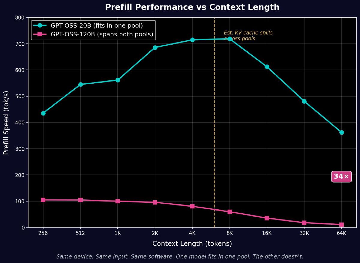
The same KOL footage also benchmarks GPT-OSS-20B (21B total, 3.6B active, MoE) on the exact same device. At INT4 that’s about 10.5 GB of weights — small enough to fit in a single memory pool.
GPT-OSS-20B at 65K context:
Prefill: 49,734.4ms @ 362.1 tok/s
Decoding: 2,992.7ms @ 10.69 tok/s
Total: 52.997s
Input tokens: 49,734.4 ms × 362.1 tok/s ÷ 1,000 = ~18,009 tokens. Same input size.
| GPT-OSS-20B (one pool) | GPT-OSS-120B (two pools) | Ratio | |
|---|---|---|---|
| Input tokens | ~18,005 | ~18,005 | Same |
| Prefill time | 49.7 sec | 1,698.5 sec | 34× slower |
| Prefill tok/s | 362.1 | 10.6 | 34× slower |
| Decode tok/s @ 65K | 10.69 | 4.47 | 2.4× slower |
| Total time | 53 sec | 1,706 sec | 32× slower |
If this were a compute difference, the 120B should be about 1.4× slower (5.1B vs 3.6B active params). If it were a bandwidth difference, maybe 2–3×. Instead it’s 34× slower on prefill. Same device, same input, same software. The only variable is whether the model crosses the pool boundary.
The KV Cache Spill Point
The prefill degradation curve tells us exactly where the split architecture kicks in. GPT-OSS-120B’s KV cache at hidden dim 2880, 36 layers, FP16:
2 (K+V) × 36 layers × 2,880 dim × 2 bytes ≈ 0.4 MB per token
| Context | KV cache size | 120B Prefill tok/s | 20B Prefill tok/s |
|---|---|---|---|
| 256 | ~100 MB | 104.7 | 435.3 |
| 4,096 | ~1.6 GB | 80.5 | 714.5 |
| 8,192 | ~3.2 GB | 59.6 | 718.6 |
| 16,384 | ~6.4 GB | 35.4 | 612.1 |
| 65,536 | ~25.6 GB | 10.6 | 362.1 |
The 120B cliff steepens around 4K–8K context — exactly where the growing KV cache starts exceeding the free space in the SoC’s 32GB pool and spilling across the PCIe boundary.
The 20B peaks around 4K–8K and then declines more steeply from 16K onward. The 20B model weighs about 10.5 GB at INT4, and its KV cache (hidden dim 2880, 24 layers) grows at roughly 0.27 MB per token. At 64K context that’s about 17.7 GB of KV cache. If the 20B runs on the SoC’s 32GB pool, model weights plus KV cache at 64K hits ~28 GB — right at the edge of usable capacity. The degradation pattern is consistent with memory pressure building on the SoC side.
Checking the 20B’s Bandwidth Ceiling
Here’s what caught me. The 20B fits in one pool and doesn’t cross the PCIe bus. It should be a clean benchmark of what the hardware can do without the split architecture penalty.
GPT-OSS-20B: 3.6B active × 0.5 bytes = 1.8 GB per token.
At 102 GB/s (SoC memory bandwidth):
1.8 GB ÷ 102 GB/s = 17.6 ms per token ≈ 56 tok/s ceiling.
The 20B hits 29 tok/s at short context. That’s about 52% of its bandwidth ceiling. Not amazing, but reasonable — memory access patterns for MoE with 32 experts and top-4 routing aren’t perfectly sequential, and there’s always scheduling overhead.
Now compare: the 120B at short context hits 16.85 tok/s against its 60 tok/s ceiling — 28% utilization. Almost half the efficiency of the 20B, even at short context before KV cache spill becomes a factor. That efficiency gap at short context — 52% vs 28% — is the base cost of the split architecture before context scaling makes it worse.
I Tried Every Scenario. Nothing Adds Up.
At this point I tried to model every possible execution configuration to find one that explains the observed numbers cleanly. None of them do.
Scenario 1: 120B on dNPU alone, no PowerInfer, no split. 2.55 GB ÷ 154 GB/s = 16.6 ms. Ceiling ~60 tok/s. At 50% utilization, ~30 tok/s. They get 16.85. Possible but this scenario is hypothetical — the 120B at INT4 is ~60 GB and doesn’t fit in the dNPU’s 48 GB pool.
Scenario 2: 120B on NPU alone, no PowerInfer. Doesn’t fit in 32 GB either. Not physically possible.
Scenario 3: 120B split across NPU and dNPU, basic layer sharding, no PowerInfer. Each side reads weights from its local memory at local bandwidth. Effective ceiling somewhere between 40–60 tok/s depending on layer distribution. PCIe crossings add ~0.04 ms per token. At 50% utilization, should still hit 20-30 tok/s. They get 16.85 at short context — close but degrading to 4.47 at 64K is too severe for this to be the only explanation.
Scenario 4: PowerInfer — hot neurons on dNPU (154 GB/s), cold neurons on NPU (102 GB/s). TiinyAI explicitly mentions “hot NPU and cold SoC neurons” in their response, suggesting this is what they’re doing. If 80% of active weights read through the NPU at 102 GB/s and 20% through the dNPU at 154 GB/s:
Cold reads: 80% × 2.55 GB ÷ 102 GB/s = 20 ms Hot reads: 20% × 2.55 GB ÷ 154 GB/s = 3.3 ms
These can’t fully overlap because results merge per layer. Per layer: cold reads ~0.55 ms, hot reads ~0.09 ms, plus PCIe round trip ~0.01–0.05 ms. Total per layer: ~0.65 ms. Times 36 layers: ~23 ms per token. Ceiling ~42 tok/s.
At 50% utilization: ~21 tok/s. They get 16.85 at short context. That’s 40% utilization — lower than the 20B’s 52%, with the gap likely explained by PCIe synchronization overhead per layer.
This scenario is the closest match for short-context performance. But it still can’t explain the 64K collapse to 4.47 tok/s — that’s 7% of the bandwidth ceiling. The additional degradation at long context comes from KV cache spilling across pools and the PCIe synchronization cost compounding across thousands of prefill tokens.
Scenario 5: 20B with PowerInfer — hot neurons on NPU, cold neurons on CPU. Total weight reads: 1.8 GB from the SoC’s 102 GB/s pool (CPU and NPU share the same memory bus). Ceiling ~56 tok/s. They get 29 tok/s — 52% utilization. This is the cleanest scenario and has no PCIe involvement, which matches the 20B’s smoother degradation curve.
But here’s the catch: if they’re running PowerInfer on the 20B, 80% of neuron computation runs on the ARM CPU. At ~3 TOPS effective for matrix ops, the CPU might actually be compute-bound for its share of the work — but because both CPU and NPU share the same 102 GB/s memory bus, memory bandwidth is likely the dominant constraint regardless.
The PowerInfer Paradox
This is where it all converges.
TiinyAI claims PowerInfer as their core technology. Every press release, every Kickstarter response, every KOL video references it. Their Kickstarter response to the bay41 analysis explicitly mentions “hot NPU and cold SoC neurons,” confirming they’re running some version of hot/cold neuron splitting.
But PowerInfer was designed for dense models where every neuron fires every token and a 24 GB GPU can’t hold the full model. The insight was brilliant for that scenario: profile neuron activation, keep the 20% that fire most on the GPU, leave the 80% that rarely fire on the CPU.
The models TiinyAI actually runs are MoE. GPT-OSS-120B has 128 experts per layer with 4 active per token — 3.125% activation. The model’s own expert router already handles sparsity. Only 3.125% of neurons are active, and ALL of them are “hot” by definition — the router selected them because they’re relevant to this specific token.
PowerInfer on top of MoE means: take the 3.125% of neurons that the router selected as important, then split THOSE further — 20% “hot” to the dNPU, 80% “cold” to the NPU. You’re splitting an already tiny workload across two memory buses with a synchronization barrier between them.
The result: 80% of the active weight reads go through the NPU at 102 GB/s instead of staying on the dNPU at 154 GB/s. PowerInfer actively moves work from the faster memory bus to the slower one. On dense models where the GPU was saturated, this tradeoff made sense. On MoE models where the dNPU has capacity to spare, it just makes things slower.
If they turned PowerInfer off and ran straight inference on the dNPU for models that span both pools, or on the NPU for models that fit in one pool, the bandwidth ceiling would be higher, the synchronization overhead would disappear, and there would be zero PCIe crossings for single-pool models.
The technique that’s supposed to be their breakthrough is reducing their effective memory bandwidth, adding synchronization overhead, and creating PCIe crossings that wouldn’t otherwise exist.
Three Sparsity Mechanisms, Zero Benefit
TiinyAI markets three sparsity technologies: MoE expert routing (built into the models), PowerInfer (hot/cold neuron splitting), and TurboSparse (model retraining for higher sparsity). All three are supposed to make inference faster by reducing work.
MoE already cuts activation to 3.125% of experts. PowerInfer further splits that small active set across two compute units. TurboSparse retrains models for even more sparsity. Three layers of “do less work per token” stacked on top of each other.
The per-token compute after all these optimizations should be vanishingly small. Fractions of a millisecond on any of their chips. The memory bandwidth ceiling should be the only constraint. And yet they’re hitting 28% of that ceiling at best, falling to 7% at long context.
Either the optimizations aren’t actually running, and the marketing doesn’t match the product. Or they are running, and the overhead of coordinating three sparsity mechanisms across multiple compute units and memory buses is worse than just doing straight inference. Either way, 190 TOPS of silicon, 80 GB of memory, three sparsity engines, and they can’t match a $400 GPU running vanilla llama.cpp with none of these optimizations.
What I Can’t Explain
I want to be honest about the limits of this analysis. I’ve modeled every execution scenario I can think of — straight NPU, straight dNPU, layer sharding without PowerInfer, PowerInfer across CPU and NPU, PowerInfer across NPU and dNPU. The bandwidth-based models get me in the general neighborhood of the short-context performance, but they can’t fully account for the severity of the long-context collapse or the gap between the theoretical and observed numbers.
There’s something in the implementation — the driver layer, the scheduling overhead, the KV cache management, the clock domain synchronization, or something else entirely — that’s burning performance beyond what any architectural model predicts. The 34× prefill gap between 20B and 120B at 65K context is too large to be explained by bandwidth ceilings alone, even with the PowerInfer penalty and PCIe overhead included.
When you can’t explain the performance gap even after accounting for every architectural limitation, every bandwidth ceiling, every bus crossing, and every software overhead — the remaining explanation is that the implementation is fundamentally broken in ways that aren’t visible from the outside. And that’s not something a firmware update fixes.
What TiinyAI Actually Proved
TiinyAI set out to debunk the PCIe bottleneck. In the process they confirmed the split memory, confirmed 8 GB/s PCIe Gen4 x4, confirmed the activation transfers at layer boundaries, confirmed the per-pool bandwidth numbers, and confirmed hot/cold neuron splitting across the SoC and dNPU.
They were technically right about one narrow thing: 8 GB/s raw bandwidth is sufficient for small activation transfers. But the split architecture creates a coordination pattern that wastes 72–93% of available memory bandwidth. PowerInfer routes the majority of weight reads through the slower memory bus. And something in the implementation burns performance beyond what any reasonable model predicts.
They showed their work. The work disagrees with their conclusion.
The Investigation
I wanted the TiinyAI Pocket Lab to be real.
A few months ago I got burned by NVIDIA’s DGX Spark, a $3,999 “personal AI supercomputer” with one fatal number buried under the marketing pile: 273 GB/s of memory bandwidth. I wrote about that here. The short version is simple: the specs sounded insane, the actual architecture was kneecapped, and I sold it at a loss.
That experience changed how I read hardware pitches. I stopped looking at the headline numbers and started looking for the missing ones. The stuff companies hide is usually the stuff that matters.
So when TiinyAI showed up claiming a pocket-sized device could run a 120B model at 20 tokens per second for $1,299, my bullshit detector lit up like a Christmas tree. I opened a text editor, pulled up their site, their renders, their prototype photos, their spec sheet, and started doing the math.
What I found looks a lot less like a miracle and a lot more like three layers of technical misdirection wrapped around forked academic research, shipped through a company that seems allergic to naming the people behind it, and sold through a Kickstarter that has now pulled in $1.7 million from 1,266 backers.
Let’s get into it.
Part 1: The Promise
TiinyAI’s pitch is clean and seductive: a pocket-sized AI supercomputer that plugs into your laptop over USB-C, carries 80GB of LPDDR5X, combines a 30 TOPS on-chip NPU with a 160 TOPS external NPU, and runs models up to “120 billion parameters” locally. No cloud. No GPU. No subscriptions. Private, offline, always on.
The Kickstarter launched March 11, 2026. It crossed $1 million in about five hours. As of this writing it sits at $1,737,722, or 17,377% of its $10,000 goal. Early bird pricing lands at $1,399, or $1,299 if you paid their site deposit in advance. Delivery is estimated for August 2026.
They have a Guinness World Record for the “smallest mini PC (100B LLM Locally).” They had a CES 2026 booth. Their press release quotes a GTM Director talking about “edge-cloud synergy” and a new product category called “AgentBox.”
And the media ate it up. Mashable, TechRadar, WCCFTech, Benzinga, Geo News. Same claims, same numbers, same zero-effort due diligence. Nobody asked what silicon was inside. Nobody asked how 120B on LPDDR5X was supposed to work. Nobody spent five minutes checking who this company actually is.
TiinyAI now lists those articles under a “Trusted by Top Media” banner on its own site. That should tell you everything about how modern hardware credibility gets manufactured.
I did the math instead.
Part 2: The Hardware They Won’t Name
The first giant red flag: TiinyAI never tells you what SoC is inside the device.
That is weird as hell. Every real hardware company names its silicon. Apple says M-series. NVIDIA says GB10. Qualcomm says Snapdragon. Even cheap SBC vendors tell you what chip you’re buying. TiinyAI gives you “Armv9.2 CPU,” “12-core,” and “160 TOPS dNPU,” then stops talking.
That turns out to be enough.
And to be crystal clear: every identification below comes from TiinyAI’s own public materials. Their renders. Their prototype shots. Their exploded views. Their spec sheet. Nobody leaked anything. Nobody disassembled anything. They showed the world the parts. I just bothered to read them.

The SoC
Armv9.2 plus 12 cores narrows the field fast.
I went through the obvious candidates:
- Snapdragon X Elite: 12-core Armv9.2, but heavily branded and Windows-centric. If they had Snapdragon silicon in the box, they’d scream it from the rooftops.
- Dimensity 9300: wrong core count.
- Apple M-series: impossible for obvious reasons.
- Ampere Altra: wrong class of chip, wrong power envelope, wrong everything.
That leaves one publicly announced production SoC that actually matches: the CIX P1 (CD8180) from CIX Technology.
Specs line up cleanly:
- 12-core Armv9.2 CPU
- 30 TOPS integrated NPU
- 128-bit LPDDR5X
- PCIe Gen4 x4 via M.2
- TSMC 6nm
My confidence here is high because there really isn’t another chip that fits the constraints.
And that matters, because the CIX P1 is not exotic silicon. It’s already shipping in boards and mini PCs. It’s a perfectly reasonable ARM chip for general compute and light AI work. Calling it a “supercomputer” is marketing cosplay.
The dNPU
The second half of the pitch is the discrete NPU: 160 TOPS on an M.2 module.
That took longer to pin down, because TiinyAI never names it either. But their own images show something important: two square dies on the NPU board. That instantly rules out a ton of common options.
The likely match is VeriSilicon’s VIP9400 architecture. VeriSilicon’s own materials describe it as scalable to 80 TOPS per core. Two cores gets you 160 TOPS. The visual geometry matches. The licensing model matches. The China-based semiconductor ecosystem match is almost too neat.
Could it be something else? Sure. Could it be a secret custom ASIC built from scratch by a seed-stage startup with no visible engineering team? Come the fuck on.
The Software Stack Points the Same Way
VeriSilicon’s toolchain uses ACUITY and TIM-VX, which helps explain several weird TiinyAI product decisions: the curated model store, the conversion pipeline, and the proprietary “Tiiny format.” Those are exactly the kinds of constraints you get when models must be precompiled against a specific NPU stack.
That means the lock-in isn’t just product strategy. It’s also architecture.
What You’re Actually Buying
Strip the marketing paint off and the Pocket Lab looks like this:
- a CIX P1 SoC
- a custom M.2 NPU module, likely based on VeriSilicon IP
- 80GB of LPDDR5X
- a 1TB NVMe SSD
- a custom enclosure
- a proprietary software stack on top
The advertised “190 TOPS” is simply 30 TOPS from the SoC plus 160 TOPS from the discrete NPU. The “bank-grade security” is AES-256 on the SSD, which is standard controller-level functionality on modern drives. That’s not product magic. That’s a checkbox.
The real story is the memory architecture, because that’s where this thing faceplants.
Part 3: The Split Memory Problem
This is the part TiinyAI almost tells you, then quietly decides not to.
Their site and Kickstarter say “80GB LPDDR5X” like it’s one big happy pool. Their own render says otherwise. It labels one side “SoC & 32GB RAM” and the other “dNPU & 48GB RAM.” The M.2 connection between them is visible in the same image.
They disclosed the split in the art, then hid it in the copy.
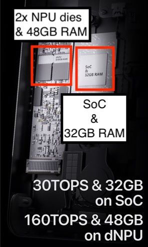
That means this device does not have 80GB of unified memory. It has two separate memory pools connected by an M.2 PCIe link.
Here’s the likely architecture:
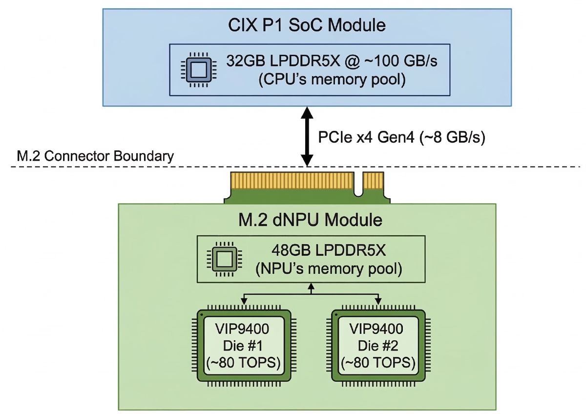
Each side probably has around 100 GB/s of local memory bandwidth. Correction (March 24): TiinyAI has since confirmed the actual figures: 102 GB/s on the SoC side and 154 GB/s on the dNPU side. The link between them is nowhere close. If this is PCIe Gen4 x4, and all visible evidence says it is, the interconnect is about 8 GB/s theoretical and more like 6–7 GB/s real.
That is the architecture in one sentence: two fast local pools, connected by a straw.
Why That Matters
LLM inference is mostly a memory bandwidth problem. Per-token speed depends on how fast the active weights and caches can be moved through the pipeline.
If a model fits cleanly inside one side of the device, local bandwidth helps. If it spans both pools, activations and state have to cross PCIe. That means your 100-ish GB/s local islands keep smashing into a 6–8 GB/s bridge.
And TiinyAI’s headline model, GPT-OSS-120B at INT4, absolutely does not fit inside the dNPU’s 48GB pool. You’re in split execution land whether you like it or not.
This is why the whole “120B at 20 tok/s” claim smelled wrong from the jump. TiinyAI wants you picturing a unified-memory wonderbox. What they actually built is a small Linux host glued to a discrete accelerator across a narrow bus.
Here’s a number that really puts this in perspective. The dNPU claims 160 TOPS at INT8. For GPT-OSS-120B with 5.1B active parameters, each token needs roughly 10.2 billion operations. At 160 TOPS, the theoretical compute ceiling is around 15,600 tokens per second. Their best measured result is 16.85 tok/s. That’s 0.1% utilization of the claimed compute. Even at a truly awful 5% utilization you’d expect 780 tok/s. They’re off by almost two orders of magnitude. Something beyond memory bandwidth is catastrophically wrong in the execution pipeline — synchronization overhead, clock domain crossings, data shuffling between three execution units that don’t share memory. This device isn’t compute-bound or memory-bound. It’s architecture-bound.
Correction (March 24): The analysis above framed the bottleneck in terms of compute TOPS. That was the wrong lens. LLM inference at this scale is memory-bandwidth-bound, not compute-bound. The relevant ceiling is how fast you can read active weights from memory per token, not how many operations the chip can perform. At 5.1B active params in INT4, that’s 2.55 GB of weight reads per token. The dNPU’s 154 GB/s gives a ceiling of ~60 tok/s — not 15,600. They hit 16.85 at short context, which is 28% of the bandwidth ceiling. Still bad, and it collapses to 7% at 64K context. The full analysis with TiinyAI’s own confirmed bandwidth numbers is in the update below.
For comparison, the DGX Spark I already trashed uses the same class of memory (LPDDR5X) at roughly 2–3× the bandwidth. On comparable MoE models at 64K context, the Spark does 15–20 tok/s with fast prefill. The Pocket Lab does 4.47 tok/s with a 28-minute TTFT. If this were purely a bandwidth gap, the performance difference would be 2–3×. Instead the TTFT gap is over 100×. That’s not a bandwidth problem. That’s the PCIe ping-pong tax on every single layer boundary, multiplied across thousands of prefill tokens.
Correction (March 24): The DGX Spark comparison still holds directionally — the Spark’s unified 273 GB/s architecture dramatically outperforms the Pocket Lab’s split pools — but the 100× TTFT gap has more nuance than I originally attributed to PCIe alone. The full breakdown is in the update.
The GGUF Filename That Gave It Away
An earlier version of TiinyAI’s desktop app showed a model file named:
gpt_oss_120b_layer_27_36.q4_0_4x64.gguf
That filename tells on them.
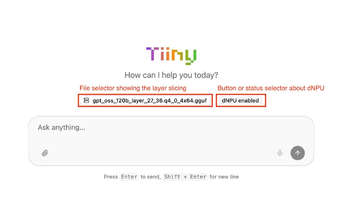
layer_27_36 strongly suggests static layer partitioning, not some magical runtime sparsity trick. The layers are preassigned. Some run on one side, some on the other. The split is baked into the artifact.
That’s important because TiinyAI leans very hard on PowerInfer in its story, and PowerInfer’s big idea is hot/cold neuron scheduling for dense models. What this screenshot suggests is much more basic: layer sharding across two memory pools because the hardware leaves them no other option.
That’s not exotic. That’s just model parallelism with extra suffering.
The Real Product Shape
The Pocket Lab is not a standalone computer in any meaningful consumer sense. It is a USB-C peripheral. Every real-world shot shows it tethered to a host machine and external power.
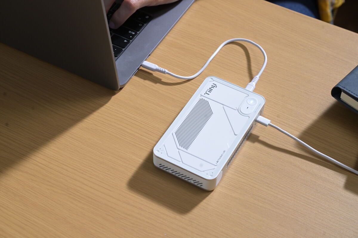
Their own developer docs expose the device over a virtual NIC and an OpenAI-compatible API. The host handles the UI, downloads, orchestration, and internet access. The device runs Linux on the ARM SoC and serves inference endpoints.
So the honest description is closer to: a Linux SBC plus NPU accelerator, exposed over USB networking, with a proprietary model store and split memory behind PCIe.
That is a real product category. It is just not the one they’re selling in the headlines.
Part 4: The KOL Videos and the Actual Performance
I never touched a unit. Almost nobody outside TiinyAI’s handpicked circle has. But right before launch, a bunch of KOL videos appeared. Influencer videos, sponsored or seeded or otherwise managed. Not independent technical reviews.
That choice alone says plenty. If this thing really did what the claims imply, you’d send it to every teardown gremlin and benchmarking goblin on YouTube and let the internet feast. TiinyAI did the opposite.
Still, the footage was useful because it exposed enough on-screen data to reconstruct what the device actually does.
First Problem: The Models Are Mostly MoE
Nearly every showcased model is Mixture of Experts. That matters because MoE headline parameter counts are not the same as active per-token workload.
| Model | Total Params | Active Params | Architecture |
|---|---|---|---|
| GPT-OSS-120B | 117B | 5.1B | MoE |
| Qwen3-Coder-Next | 80B | 3B | MoE |
| GLM-4.7-Flash | 30B | ~3B | MoE |
| Qwen3-30B-A3B | 30B | 3B | MoE |
| GPT-OSS-20B | 21B | 3.6B | MoE |
| Qwen3-8B | 8B | 8B | Dense |
That “120B” flagship model only activates about 5.1B parameters per token. Which means the device is not doing 120B dense-model work per step. It is doing something much closer to a small dense model while keeping a large MoE weight set resident in memory.
That distinction never shows up in the marketing, for obvious reasons.
Second Problem: The Benchmark Setup Is Extremely Friendly
The visible benchmark runs use 32-token outputs and tiny contexts to manufacture good-looking numbers. That’s basically a lab demo for a short sentence, not a serious workload.
Here is the GPT-OSS-120B decoding table visible in KOL footage:
| Context Length | Output Tokens | Decoding Speed |
|---|---|---|
| 256 | 32 | 16.85 tok/s |
| 512 | 32 | 16.77 tok/s |
| 1,024 | 32 | 16.43 tok/s |
| 2,048 | 32 | 15.38 tok/s |
| 4,096 | 32 | 14.42 tok/s |
| 8,192 | 32 | 12.04 tok/s |
| 16,384 | 32 | 9.16 tok/s |
| 32,768 | 32 | 6.04 tok/s |
| 65,536 | 32 | 4.47 tok/s |
Best case is 16.85 tok/s, not 20, and that’s under the most flattering possible conditions.
Once you move into context sizes that resemble actual work, the floor drops out:
- 8K: 12 tok/s
- 16K: 9 tok/s
- 32K: 6 tok/s
- 64K: 4.47 tok/s
That curve is exactly what you’d expect from a split-memory system whose nice-looking local bandwidth numbers keep running face-first into a much slower bridge.
TTFT Is a Bloodbath
The time-to-first-token numbers are even worse.
| Model | TTFT @ 256 ctx | TTFT @ 8K ctx | TTFT @ 64K ctx |
|---|---|---|---|
| GPT-OSS-120B | ~5.3s | ~75s | ~1,706s (28 min) |
| Qwen3-30B-A3B | ~26s | ~19s | ~97s |
| GPT-OSS-20B | ~1.8s | ~7.5s | ~53s |
Twenty-eight minutes to first token at 64K context.
That is a completely deranged number for something marketed around coding, RAG, and agent workflows. Those are exactly the workloads that build context over time. Once you hit 16K, 32K, 64K, you’re no longer dealing with a cute inconvenience. You’re dealing with a product that turns every iteration loop into a hostage situation.
Real-World Demos Weren’t Reassuring Either
The coding demos were toy-tier: HTML, CSS, and JavaScript, single-file stuff, heavily edited, with prefill and thinking time regularly fast-forwarded or cut around. One “3D flight game” demo produced a floating box with controls after an eternity of inference. Nobody threw a real repo at it. Nobody ran meaningful long-context code assistance. Nobody benchmarked the product against actual local GPU rigs at comparable price points.
Because if you did that, the story would fall apart fast.
For perspective: a consumer NVIDIA RTX 4060 Ti (~$400) can run comparable 3B active-parameter MoE workloads at 70–90 tok/s with 100K+ context, depending on setup. The Pocket Lab lands around 6–12 tok/s at 8K–32K context.
Same class of workload. Roughly 5–10× slower, at 3× the price, with tighter constraints.
Part 5: The “120B” Sleight of Hand
This is the core marketing trick.
TiinyAI advertises “120B” everywhere because that’s the number that looks impressive. But GPT-OSS-120B is a Mixture of Experts model with 5.1B active parameters per token.
That means the per-token work is closer to a small dense model, not a dense 120B monster. The full 117B still needs to live somewhere, which is why the 80GB memory number matters. But the speed claim only makes sense because the active compute footprint is much smaller than the headline implies.
TiinyAI never leads with that. They rarely even say “MoE.” They definitely do not explain active parameters in the headline pitch.
And that omission isn’t some harmless simplification. It’s the entire trick.
Part 6: The PowerInfer Story
TiinyAI also leans on PowerInfer and TurboSparse as if these are proprietary secret weapons.
They’re not.
PowerInfer came from the IPADS lab at Shanghai Jiao Tong University. The original paper landed in late 2023. TurboSparse followed in 2024. Real researchers. Real papers. Real contributions.
The important distinction:
- PowerInfer is a runtime inference technique built around dense-model activation sparsity. It profiles which neurons fire frequently across typical inputs, preloads those “hot” neurons onto the GPU, and leaves the “cold” ones on the CPU. The key detail: this profiling works because dense models have predictable, stable neuron activation patterns.
- TurboSparse is a model-side sparsification approach that can also apply to MoE settings.
TiinyAI blurs those together constantly. That matters because the story they push hardest, hot neurons and clever scheduling, is the one that fundamentally doesn’t apply to their demo lineup. MoE models already have their own sparsity mechanism: the expert router picks which experts fire at runtime, per token. You don’t know in advance which experts will activate — that’s the whole point of mixture-of-experts. Trying to layer PowerInfer’s neuron-level predictions on top of MoE’s expert-level routing is redundant at best: the routing already decides which parameters are active.
What the product appears to rely on in practice is a mix of NPU-specific compilation, static sharding, and curated model packaging. That’s a lot less magical than the research-branding suggests.
Part 7: The Attribution Problem
TiinyAI’s Kickstarter timeline claims:
- Jan 2024: Team founded
- Jun 2024: Launched the open-source projects PowerInfer and TurboSparse
That timeline is cute, except PowerInfer was published in December 2023, before TiinyAI supposedly existed.
So no, TiinyAI did not “launch” PowerInfer. SJTU researchers did.
TiinyAI’s GitHub repo is a fork of the original PowerInfer repository. At least one of the original academic authors appears tied to the code history. So there is clearly some real overlap between the research world and the product world.
But the public framing still matters, and the framing here is slippery as hell. Academic work became product branding, the original repo path now redirects, and the commercial narrative gives TiinyAI far more ownership over the origin story than the timeline supports.
Oh, and their PR Newswire press release describes PowerInfer and TurboSparse as “Tiiny AI’s proprietary optimization technologies.” Proprietary. For code that’s on a public GitHub repo under an open-source license. The fork’s only notable modification was editing the README to add a product announcement.
That’s a forked academic project turned into startup mythology.
Part 8: The Corporate Opacity
Now for the part that gets genuinely sketchy.
If you had really built the world’s smallest AI supercomputer, your leadership team would be everywhere. CEO. CTO. Chief scientist. Founder story. Conference clips. Interviews. LinkedIn profiles. The usual startup peacocking.
TiinyAI has basically none of that.
What I found publicly was a tiny, weird footprint:
- a hidden VP in Dover, Delaware, name behind LinkedIn’s paywall, reverse image search turns up nothing
- a GTM Director with almost no visible career history — and a name that doesn’t quite match. TiinyAI’s press releases all quote “Samar Bhoj, GTM Director.” The LinkedIn profile for the same title, same company, same location reads “Satyendra B.” The “B” could stand for Bhoj, making them the same person using different names on different platforms. Or they’re two people sharing the same title at a four-person company. Either way, the single most visible human in the organization can’t maintain a consistent identity across platforms.
- a Hong Kong VC analyst at Gobi Partners listing TiinyAI as a portfolio company
- a Hong Kong intern with a pixel art avatar
That’s not a normal public surface area for a company allegedly shipping breakthrough AI hardware, raising a seed round, setting Guinness records, and pulling in $1.7 million on Kickstarter.
The Gobi Partners connection is worth pulling on. Gobi runs the Gobi-Redbird Innovation Fund, which exists specifically to commercialize HKUST research. TiinyAI claims team members from HKUST. The fund’s own press materials name Lymow — the same Lymow that shows up alongside TiinyAI in the analyst’s portfolio. The “multi-million dollar seed round from leading global investors” that Crunchbase won’t name almost certainly came through this pipeline.
The geography tells its own story. The silicon trail points to Shenzhen and Shanghai. The research trail points to SJTU. The PR trail runs through Hong Kong (their press release carries distribution code HK08267 — a Hong Kong wire release, syndicated globally through PR Newswire to create the appearance of widespread coverage). The visible investor connection points to Hong Kong. The company presents as a U.S. AI infrastructure startup out of Delaware.
Could all of that still be technically true? Sure. Delaware shells are cheap. Global hardware supply chains are normal. Chinese silicon is not a crime. None of that is the problem.
The problem is the pattern. Every thread that would help a buyer understand who built this, who funds it, who stands behind it, and who will still exist if things go sideways is either blurred, missing, or redirected through a marketing layer.
That is not how trust gets built. That’s how responsibility gets diffused.
Part 9: The Kickstarter Math
The $10,000 campaign goal is its own joke.
A custom hardware product with:
- 80GB of LPDDR5X
- a custom NPU module
- PCB work
- enclosure tooling
- thermal engineering
- certification
- manufacturing
- logistics
does not get brought to market for ten grand unless the plan is to print one very expensive prototype and call it a day.
The goal is fake. It exists to generate a giant “% funded” number and make the campaign look like a runaway phenomenon. Real hardware costs were obviously coming from somewhere else long before Kickstarter went live.
And that circles back to the biggest concern: if the company structure is already opaque, and the public-facing leadership is basically nonexistent, what exactly happens if this campaign slips, pivots, stalls, or dies?
Kickstarter backers are not buying a product off a shelf. They’re funding a promise made by a corporate shell with unusually few visible humans attached to it.
That’s a bad combo.
What an Honest Product Page Would Say
Here’s the version I wish TiinyAI had published:
Portable USB AI inference accelerator. Runs selected MoE models with up to 120B total parameters, but much smaller active per-token workloads, at roughly 12–16 tok/s under short-context conditions. Longer contexts degrade sharply, with roughly 6–9 tok/s in the 8K–32K range and very high TTFT at 32K+. Requires host computer and proprietary desktop software. Uses split memory architecture across a 32GB SoC pool and 48GB dNPU pool connected over PCIe. Model support is limited to pre-optimized builds from TiinyAI’s store. Inference stack builds on PowerInfer research from SJTU IPADS.
That would still be a real product description. It would also be a much harder sell for $1,399.
And that’s the whole point.
Final Thoughts
I don’t think this is pure vaporware. The device appears to exist. It appears to run models locally. The CIX P1 is real. VeriSilicon IP is real. PowerInfer is real. MoE models are real. You can absolutely assemble something that sort of does what they’re showing.
What I do think is that the pitch is systematically misleading.
They push “120B” without explaining active parameters. They advertise 80GB without clearly explaining the split pool. They quote impressive local compute numbers while avoiding the architectural bottleneck joining the two halves of the system. They lean on academic research they did not originate. They present as a U.S. startup while the visible technical and operational trail runs heavily through China and Hong Kong. And they ask backers to fund all of this without clearly naming the people responsible for delivering it.
That’s too many omissions in exactly the places an informed buyer would want details.
I wanted this thing to be real. I wanted somebody to have cracked portable local inference at a sane price point.
The physics didn’t budge. The architecture still sucks. And the math does not give a shit about the Kickstarter video.
All hardware identification in this post was derived from TiinyAI’s own public marketing images, social posts, renders, prototype photos, spec sheets, press releases, and Kickstarter materials, along with public academic papers, GitHub repos, LinkedIn profiles, corporate records, and DNS data. No proprietary or leaked information was used. No device was obtained, tested, or disassembled.
I have no financial position in or relationship with TiinyAI, CIX Technology, VeriSilicon, Gobi Partners, or any other entity mentioned here. I did not back the Kickstarter.